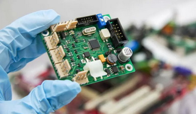
Al Technology-Electronic Design and Manufacturing

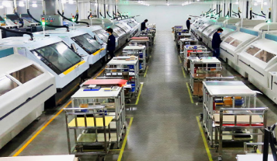
The integration of artificial intelligence (AI) in electronic manufacturing services has grown quickly in the industry. In PCB manufacturing, AI is used to carry out different tasks, and this has made the production process easier and more The integration of artificial intelligence (AI) in electronic manufacturing services has grown quickly in the industry. In PCB … Continued

Advanced heavy copper PCB manufacturer

Must knows to heavy copper PCB and it’s manufacturers

What is the heavy copper PCB Usually, when out-layers or inner-layers of any printed circuit board are specified to use ≥2oz base copper foil, we call it heavy copper PCB (or thick copper PCB board). For final finished copper thickness (means base copper + plating copper) we normally follow customers’ requirements to do.But,if no specific … Continued

Advanced PCB manufacturer

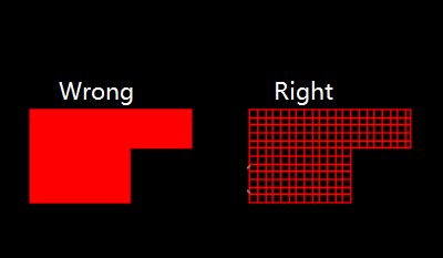
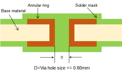
Guidelines to via holes treatment method in PCB design

When you finish your PCB layout design and then you can send it to PCB manufacturers who provide custom circuit board service to have your PCB board manufactured. And, you can plan your final electronic PCB assembly after custom circuit board printing process finished. The engineering flow process before manufacturing electronic PCB Normally, the designer … Continued

China PCB Prototype & Fabrication Manufacturer

How to Choose the Best PCB fabrication Manufacturer

Nowadays,PCB manufacturing is hot competitive, and there is lot of worldwide manufacturing capacity factories for any technology challenge circuit boards. If you’re ready to look for a professional PCB manufacturer for your next project, more or less it can be difficult to determine who is the best option to produce your circuit board. Different PCB fabricators … Continued

PCB-layer-stackup-design

How to specify PCB layer orientation in PCB design.

To perform the correct PCB production of your printed circuit board, it must have a label in the copper of the PCB top and PCB bottom layer, for multilayer PCB additionally on the inner layers. In China, it was once common practice to label the Component Side (assembly side) with BS, and the solder side … Continued

PCB copper balance design and layout

How to understand PCB Copper balance in PCB fabrication

A symmetric copper distribution (copper balance) on the circuit board is very important, because asymmetric copperleads to bow and twist effects in PCB fabrication process,and finally will affect the soldering quality of components in PCB assembly process. This warping of the form is caused by thermal loads in the circuit board, such as those caused … Continued

PCB panel design and manufacturing

How to design couple of different PCBs in one panel

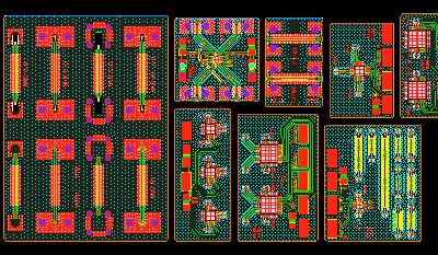
Optimize the global manufacturing cost of PCB and PCBA prototypes When it comes to start a PCB design for prototypes, Most circuit board designers like to put various PCBs (the same layer count and stack up but with difference in size, shape etc) into one panel to optimize the cost in the PCB fabrication and … Continued

controlled-impedance-PCB-manufacturer

What is the PCB impedance coupons

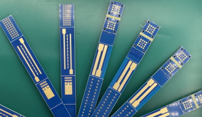
The brief summary about PCB impedance PCB board with controlled impedance trace is very important for signal transmission quality.Especially for quick switching parts with signal rise times of 1 to 2ns, the signal integrity must be guaranteed through good impedance characteristics in the conductor trace connections. What is the PCB impedance coupons The PCB impedance … Continued

16-layers-pcb-manufacturer

Standard 16 layer PCB stackup options

Our standard 16L layers stackup is the most common options selected by most PCB designers. The standard 16 layer stackup can be utilized in most applications for multilayer PCB board. As the standard options, you can get a variable 16 layer stack up from Weller’s engineering suggestion, which is defined by following with 3 options … Continued