What is the PCB embedded copper coin.
The PCB embedded copper coin is the copper coin embedded in the PCB Cavity or slot after routing and metalized when finished PCB lamination. PCB and it’s copper coin tightly connected.
The purpose of using PCB copper coin embedded technology.
The traditional way to dissipate heat in a printed circuit board is through thermal vias holes. But most PCB material is not particularly good for heat transfer.On other hand, some crucial components need high performacne of heat dissipation which standard via holes can not meet.
Copper, on the other hand, is an excellent conductor of heat, which is why adding copper coin to your PCB is highly effective when you need to dissipate heat from an active PCB.
With PCB embedded coin technology, you can insert a piece of copper coin directly under the component to absorb and dissipate excess heat. T-Coin, I-Coin and C-Coin refer to the shape of the coin which you will be using, based on the shape of the area where you are trying to offset the excess heat.
The methods of dissipating heat for PCB
Normally, there are 3 methods to dissipate the head for printed circuit board.
| 1. Via holes filled by resin (Via in PAD) |
| Specification to holes: 1. Via hole size: 0.2-0.4mm 2. Though via holes 3. Via holes plugged by resin and copper plating over on top and bottom side. |
| 2. Via holes filled by copper |
| Specification to holes: 1. Through via hole size: 0.3-0.4mm 2. Blind via holes: 0.10mm 3. Through via holes or blind via holes fully filled by copper. |
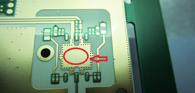
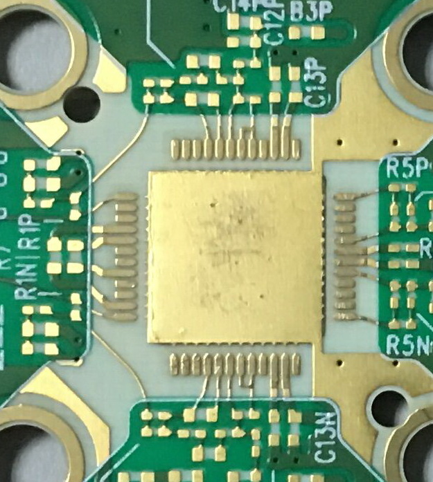
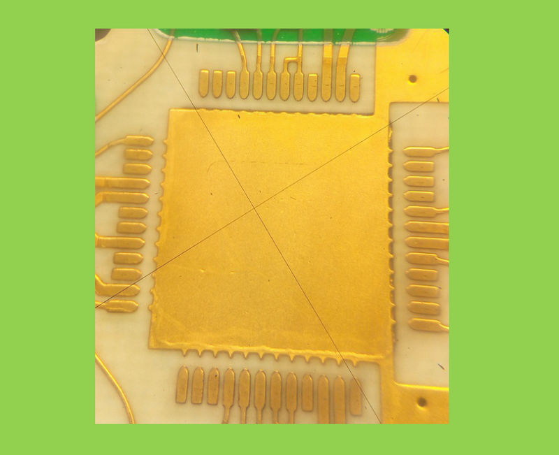
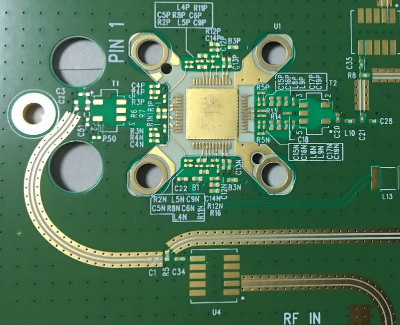
| 3. Cavtiy or routing zone embedded by copper coin |
| Specification to Copper coin: Size: 3.000 X 3.00mm (min); 60.00 X 80.00mm(max). Copper coin thickness: 1-3mm PCB Surface finishing: immersion gold.(must be this). |