Optimize the global manufacturing cost of PCB and PCBA prototypes
When it comes to start a PCB design for prototypes, Most circuit board designers like to put various PCBs (the same layer count and stack up but with difference in size, shape etc) into one panel to optimize the cost in the PCB fabrication and PCB assembly. This is a good idea for PCB prototypes and PCB turnkey assembly as the time and cost saved much.But most designers do not have a good concept that how to optimize their boards in the panel as this is a accurate and professional work that the CAM engineers in the PCB house is good at.
How to design various of PCBs in one panel
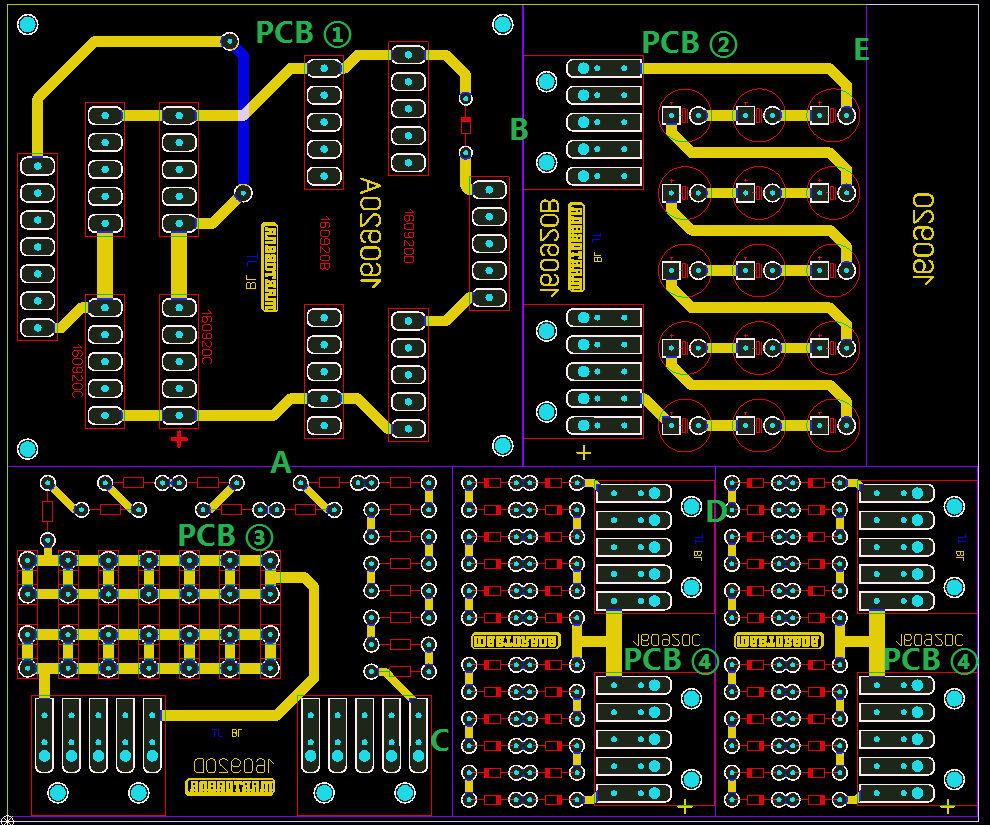
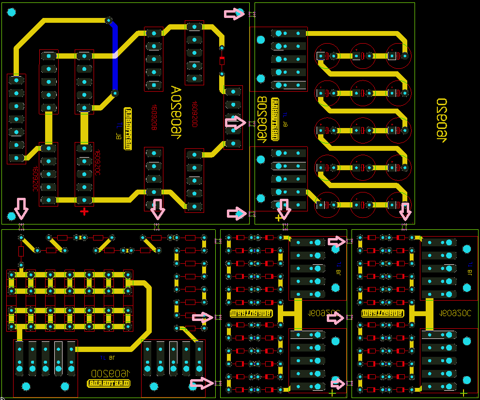
Apparently it looks like an easy work to PCB designer or PCB layout engineers but actually not. See below picture which is a PCB penal with 4 different of PCBs (PCB①,②,③,④)from the original PCB layout engineers. It is a good idea but it cannot come out to the PCB fabrication factory as the connection between each PCB is simply fixed by V-CUT line(Totally is 5 V-CUT lines (A,B,C,D,E)). Only V-CUT “A” can work out as it is a continues V-CUT line. All other 4 V-CUT lines cannot work as the each single PCB board will be scraped when perform V-CUT process.
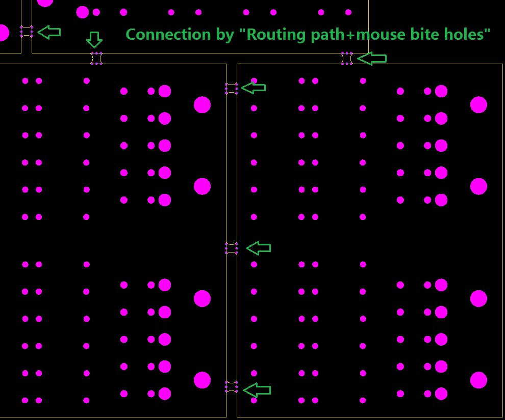
If the single PCB has un-regular shapes, the best option to design the panel is to make the connection by routing + mouse bites holes, as model picture below(2.0mm routing path+0.5mm mouse bite holes to hold the single PCB):
The basic cores that generating the PCB fabrication panel
To combine various PCB in one panel, the basic condition is that each PCB should have the same specification below:
- Layer count
- Base material
- Copper thickens
- Surface finishing
- Same color so solder mask
- The color of silkscreen
- Not for HDI PCB boards.
- The singld PCB size can not be too large
- No impedance for multilayer PCB(as impedance will affect the stack up)
The 2 must knows to combine the different PCBs in one panel assembly
- The designator (component name) cannot be duplicated with each other, must be listed by the numerical order,:such as C1,C2..C10 in PCB①, and C10,C11….C50, in PCB②…etc)
- The pack and place file must be listed in the same panel file by the numerical order as the panel of BOM.
If you have any more questions about different PCBs designed in one panel, please contact us freely by [email protected].