To perform the correct PCB production of your printed circuit board, it must have a label in the copper of the PCB top and PCB bottom layer, for multilayer PCB additionally on the inner layers.
In China, it was once common practice to label the Component Side (assembly side) with BS, and the solder side with TS. With SMD assembly this is no longer appropriate, and even worse, in a technical environment where English is more common, the abbreviation “BS” may be misunderstood as “bottom side”! We therefore recommend a uniform inscription using TOP and BOT (for ALL languages!), to indicate the upper and lower sides.
Please NOTE: missing or incorrect labelling is the most frequent cause of problems, since many PCB Layout programs permit mirrored data output! For this reason, please label your circuit boards always with TOP and BOT in the copper! Correct labelling with TOP and BOT in the circuit board’s copper provides information about the PCB layer definition, and also for the layer orientation!
PCB layer definition = unique labelling of top and bottom layers.
PCB layer orientation = labelling to avoid mirrored layers.
Problems with PCB layer orientation
Even when your data uniquely defines which layer the top bottom layer is, the layer orientation cannot be determined without an inscription in the copper, since nearly every CAD program permits a mirrored output of the data (this is even true for single-sided circuit boards).
Note: This is not a special case just for Multi PCB, it applies worldwide for every printed circuit board manufacturer.
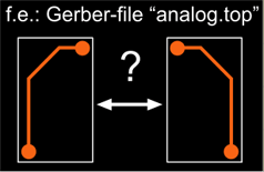
This is the TOP layer of a circuit board. Which (layer) orientation is correct (right or left)?
Correct layer orientation
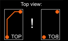
In your layout program, the label should appear in the copper as shown in the diagram. As seen from above, the word “TOP” should be legible, the label “BOT” for the bottom layer should be mirrored.
Important: do not mirror the data output!
BOT will be legible once the circuit board is complete.
Layer definitions for multilayer
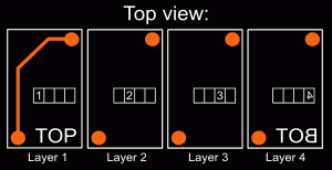
For multilayer PCB, we recommend a continuous label for the layers, as shown in the diagram.
Once again, here it is important that the label (inclduing all the silkcreen letters,logos,etc) for the bottom layer appears mirrored when viewed from above.
The captions “layer 1” to “layer 4” are shown only for clarity