What is the heavy copper PCB
Usually, when out-layers or inner-layers of any printed circuit board are specified to use ≥2oz base copper foil, we call it heavy copper PCB (or thick copper PCB board).
For final finished copper thickness (means base copper + plating copper) we normally follow customers’ requirements to do.But,if no specific finished copper thickness from PCB designer, we will follow IPC standard(usually Class 2) to control. For example (inner layers 2oz base copper, the finish thickness is 55.7um; outer layers 2oz base copper, the finish thickness is 78.7um).
The advantages of heavy copper thickness PCB
The heavy copper’s advantages: increased endurance to thermal stress, reduce product size, increased current carrying capacity, flat planer transformer, smaller ecological footprint,etc.
The lead time of heavy copper thickness PCB manufacturing
As the heavy copper raw materials are not commonly used as standard copper thickness raw material, so normally circuit board manufacturers do not regularly have this type of material in stock (specially the copper thickness >= 4oz). And standard lead time to purchase it from 1-4 weeks or more after receiving your purchase order. That means you need to plan it beforehand when you need to order the heavy thickness copper PCB from a thick copper PCB manufacturer.
However, electronic board manufacturers normally have some common thick copper material in stock (such as 2oz,3oz, 0.8mm, 1.0mm,1.60mm) for 2 layers heavy copper PCB.
The characteristic of heavy copper thickness PCB
Due to it’s better thermal conductivity characteristics,the heavy copper PCB often require high grade of PCB raw material with high TG(TG≥) 170 to ensure it no de-lamination or no blister in multi-layer PCB manufacturing process.
Since it’s “heavily” copper thickness, the etching production process is becoming much more harderthan normal etching prduction process. It required longer time for etching and the trace side etching will be increased accordingly.The trace width size need to be designed more wider. Also the trace need to be compensated more in order to balance the etching loss (below chart for copper thickness with corresponding trace width/spacing needed).
It is better to design copper area evenly on board, for etching the bigger spacing area often easier than narrower spacing area. The uneven copper may make trace tolerance hard to control. What’s more, if the bigger copper free area at same place on every layer, it has the risk of enlarging board board thickness extreme value and cause dry file pasted not tightly, which will make the boards scraped.
The circuit track width for heavy copper thickness PCB design
When you start a heavy copper PCB design, it is better to follow below specification to perform the PCB layout in circuit track width/spacing
| Outer layer Cu base weight (OZ) | Minimum track spacing (mil/mm) | Minimum track width(mil/mm) |
| 0.33 | 3.50/0.089 | 3.00/0.08 |
| 0.50 | 4.00/0.10 | 3.50/0.089 |
| 1.00 | 6.00/0.15 | 5.50/0.14 |
| 2.00 | 9.00/0.23 | 9.00/0.23 |
| 3.00 | 13.00/0.33 | 13.00/0.33 |
| 4.00 | 17.00/0.43 | 17.00/0.43 |
The stackup design of heavy copper thickness PCB
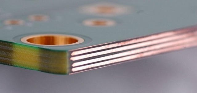
The lamination process is one of critical processes in multi-layer heavily copper PCB production. The lamination procedures for multi-layer heavy copper PCB is different from that in the standard multi-layer PCB. Thus,the stack up design for multi-layer heavy copper PCB is very important to make sure the best quality in it’s electric function and facilitate in manufacturing.
In order to fill the spacing being etched off,it needs a lot of resin to fill in the gaps of copper etched out. Usually the resin needed is from the prepreg in lamination process. Something below need to be attentioned when you start a stack up design for a multi-layer heavy copper PCB:
It is better to try to reduce the copper area differences between the symmetrical layers can be very helpful to control the PCB warpage. (e.g. for 8L PCB, the symmetrical layer is:L2&L7 or L3&L6 or L4&L5 or L1&L8 ).
To avoid preprge starved after laminating process:
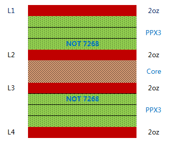
If the inner layers copper thickness is >=2oz, the stack-up design will require the prepreg 7628 to NOT close to the inner 2oz copper.
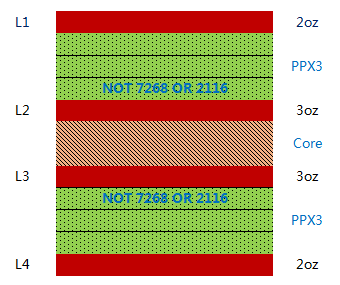
And if the inner layers copper thickness is >=3oz, the stack-up design will require the prepreg 7628 or 2116 NOT to be close to the inner 3oz copper,as 7628 or 2116 is the low resin content PP.
Also, Usually as it require more PCS of Prepreg (also called PP) between the heavy copper layers. So sometimes it come out some little problems for heavily copper PCB lamination:
1.The total thickness will become high.If the prepreg used too less,it may cause the void inside the layers after PCB lamination process. But too many prepreg may cause the total thickness too high or dielectric thickness between layers out of specification;
2. During lamination, the multiple high resin content prepreg will have high resin flow and will cause the inner layers shift. The layer-to-layer mis-registration will become another problem accordingly;
3. The resin rich area may have resin crack issue for its no reinforcement. The higher CTE raw material also cause some reliability issue in higher temperature.
The drill holes design for heavy copper thickness PCB
When the PCB design has many thick copper layers, the drilling parameter need to be adjusted to more similar to drill a thick copper plate. The drill bit wear and debris removal need to be process carefully. It is better to removal inner layers isolated pads, else, it is need to enlarge the isolated pad enough big to avoid copper pulled off when drilling.
The soldermask design for heavy copper thickness PCB
PCB Soldermask print is another issue for heavy copper PCB.It’s difficult to apply enough soldermask to cover thick copper pattern and base material with severe height difference. Usually,PCB manufacturers need to fill more solder mask to fill in the spacing between the trace.
It’s common to apply multiple printing. The first printing fill most of the pattern gap and second printing cover enough thick of soldermask on the trace pattern. But it still have some risk of voiding. The thick soldermak is also more difficult to exposure and develop. If the exposure energy is too weak, then some undercut problem may happen.
If you have a complex muti-layer heavy copper PCB in design process and ready to look for high quality of heavy copper PCB manufacturers, you can contact us by [email protected], our engineer can support you by DFM service to ensure your design at economic cost and facilitate in manufacturing process.