
WellerPCB has over 10 years experience in PCB design. We can use our extensive PCB design capability to handle your layout overflow in time of need.
We offer a full range of PCB layout services for your new boards as well as changes to existing boards.
- Tools for layout: ORCAD, PADS (Power PCB), Allegro 15.5, 15.7, 16.3, 16.3
- PCB layout from schematic capture to preliminary parts placement through the final routing
- Customers will be provided with check plots to keep them apprised of the progress.
Experiences and Capabilities
Notebook, Desktop PC
Server,IPC
Router, Switch Hub, Wireless Router
Mobile Phone,Smart Phone,GPS
Video products
All analog, high speed digital,and mixed signal PCB layout
Multilayer, impedance controlled design
Short-range and long-range wireless products
Ultrasonic,optical,and radar products
Embedded systems design,including software development with standard COMs

For correct PCB production of your printed circuit board, it must have a label in the copper of the PCB top and PCB bottom layer, for multilayer PCB additionally on the inner layers.
In China, it was once common practice to label the Component Side (assembly side) with BS, and the solder side with TS. With SMD assembly this is no longer appropriate, and even worse, in a technical environment where English is more common, the abbreviation “BS” may be misunderstood as “bottom side”! We therefore recommend a uniform inscription using TOP and BOT (for ALL languages!), to indicate the upper and lower sides.
Please NOTE: missing or incorrect labeling is the most frequent cause of problems, since many PCB Layout programs permit mirrored data output! For this reason, please label your circuit boards always with TOP and BOT in the copper! Correct labeling with TOP and BOT in the circuit board’s copper provides information about the PCB layer definition, and also for the layer orientation!
PCB layer definition = unique labeling of top and bottom layers.
PCB layer orientation = labeling to avoid mirrored layers.
Problems with PCB layer orientation
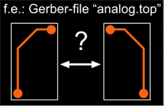
Even when your data uniquely defines which layer the top or bottom layer is, the layer orientation cannot be determined without an inscription in the copper, since nearly every CAD program permits a mirrored output of the data (this is even true for single-sided circuit boards).
Note: This is not a special case just for Multi PCB, it applies worldwide for every printed circuit board manufacturer.
This is the TOP layer of a circuit board. Which (layer) orientation is correct (right or left)?
Correct layer orientation
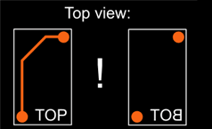
In your layout program, the label should appear in the copper as shown in the diagram. As seen from above, the word “TOP” should be legible, the label “BOT” for the bottom layer should be mirrored.
Important: do not mirror the data output!
BOT will be legible once the circuit board is complete.
Layer definitions for multilayer PCB design
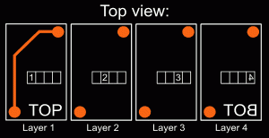
For multilayers PCB, we recommend a continuous label for the layers, as shown in the diagram. Once again, here it is important that the label for the bottom layer appears mirrored when viewed from above.
The captions “layer 1” to “layer 4” are shown only for clarity.
Powered by China Printed Circuit Board manufacturer (offshore PCB Manufacturers and Turnkey PCB assembly manufacturer)
If you have any question in thje beginning of your PCB design for your creative project to facility of PCB manufacturing,please contact our technology consultor: [email protected].