When you finish your PCB layout design and then you can send it to PCB manufacturers who provide custom circuit board service to have your PCB board manufactured. And, you can plan your final electronic PCB assembly after custom circuit board printing process finished.
The engineering flow process before manufacturing electronic PCB
Normally, the designer provides PCB Gerber and extra manufacturing specification document to manufactures for a better guideline to manufactures.
Firstly, the PCB manufacturer will review the electronic PCB purchase order with Gerber files and some special requirements for manufacturing specification document (If any).
Secondly, the engineers from PCB board house will perform regular DFM review such as “surface finishing, minimum via holes size, minimum track width/spacing, and whether customer’s PCB stackup is upon standard PCB thickness or not, etc”.
In this article we will focus on talking about the Via holes design issue frequently asked by manufactures.
So, it is very important to you to have your Gerber design match the information in your manufacturing specification document. Any mis-matched information will questionnaire the PCB manufacture’s engineer. Such as ” In the Gerber data, the via holes designed as solder mask plugging on both side but in your specification you require via holes to be not covered by Solder mask”
Via holes design VS different PCB surface finishing
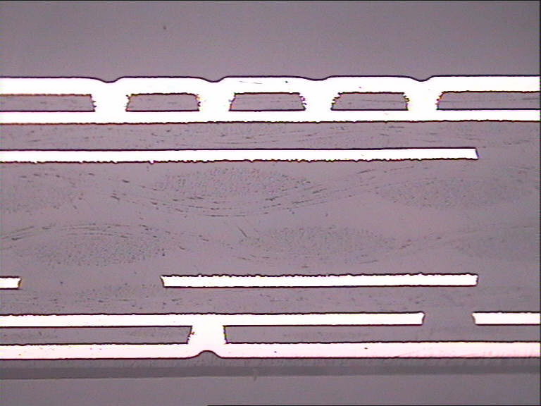
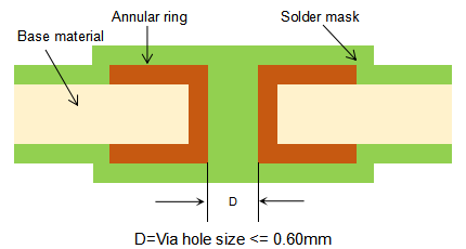
As we know via holes is usually referring to smaller size of PTH holes (generally,the via hole size are smaller than 0.6mm) to carry the conductive features in the loop of circuit diagram, which are not used for through hole components soldering.
Generally, the manufactures will be always following the designer’s original Gerber data with it’s manufacturing specification to manufacture the PCB board. Most of electronic PCB board designed as via holes plugged by solder mask (without solder mask openings on both sides) . Few of them designed as via holes with solder mask opening on top and bottom side.
The via holes are without solder mask openings both sides to all surface treatments is OK.
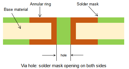
For ENIG (chemical gold/immersion gold) or OSP (Entek), it is no problem for single side solder mask openings for via holes; also no problem with both sides solder mask opening for via holes.
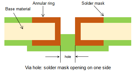
For HAL (or HAL lead-free), it is not good to design it as single side solder mask openings for via holes. Since solder from electronic PCB assembly may get trapped in holes and plug the via holes, the trapped soldering will take a potential risk of circuit shortage between via holes and tracks. If the via holes size is too small(smaller than 0.45mm), it is not good to design it as solder mask opening on both sides, as the soldering from PCB assembly process may plug the via holes, also soldering may plug the small NPTH holes(NPTH holes size smaller than 0.6mm, like the stamp holes some times are smaller than 0.6mm).
For immersion Tin or immersion silver, it is OK to design via holes as solder mask opening at both sides(top and bottom side). But it is not good to design it as single side solder mask openings (the other is plugging) for via holes, since the chemical liquid of immersion Tin or immersion Ag may get trapped in small via holes and survive to erode the hole copper, this will cause via holes lack of copper and take potential risk of open circuit.
Sometimes, there are some via holes are touched the solder mask openings pads, or partially overlapped with the solder mask openings pads. The partial older mask openings of via holes is not convenience to filling via holes with solder mask openings, and the solder mask may encroach the solder pads cause solder mask on pad,which will take extra problem to PCB assembly process. To avoid this:
If the solder mask overlapped pads smaller than 1/2 holes size, PCB manufacture house often suggest to shave the solder mask openings to get about 0.1mm away from via hole edge.
If the solder mask overlapped pads bigger than 1/2 holes size(or equals 1/2 holes size), engineers often suggest to add a whole solder mask opening(size bigger than via hole 0.1mm per side) for the via hole. If all via holes(hole size smaller than 0.7mm) are need to be filled by resin, there is no problem with all of above questions, but this increase the cost, and need extra production time (about extra 1-2 days).
Laser drilling holes on HDI printed circuit boards
If your PCB is HDI printed circuit boards with laser drilling holes in it, normally the HDI PCB manufacturer will plug the laser drilling holes filling copper and then plate copper over it to be shut up (as copper capped).