14L-rigid-PCB-stack-up-design

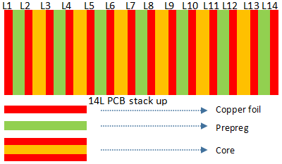
Standard 14 layer PCB stackup options

Our standard 14L layers stackup is the most common options selected by most PCB designers. The standard 14 layer stackup can be utilized in most applications for multilayer PCB board. As the standard options, you can get a variable 14 layer stack up from Weller’s engineering suggestion, which is defined by following with 3 options … Continued

12-layer-pcb-manufacturer

Standard 12 layer PCB stackup options

Our standard 12L layers stackup is the most common options selected by most PCB designers. The standard 12 layer stackup can be utilized in most applications for multilayer PCB board. As a standard option, you can get a variable 12 layer stack up from Weller’s engineering suggestion, which is defined by following : PCB thickness: … Continued

10-layer-pcb-manufacturer

Standard 10 layer PCB stackup options

Our standard 10L layers stackup is the most common option selected by most PCB designers. The standard layer stackup can be utilized in most applications. As a standard, you can get a variable 10 layer stack up from Weller’s engineering suggestion, which is defined by following : PCB thickness: 1.3mm/1.6mm/2.0mm/2.4mm/3.0mm Final finished copper thickness: 1/1/1/1/1//1/1/1/1/1oz … Continued

8-Layer-rigid-pcb-stack-up

Standard 8 layer PCB stackup options

Our standard 8L layers stackup is the most common option selected by most PCB designers. The standard layer stackup can be utilized in most applications. As a standard, you can get a variable 8 layer stack up from Weller’s engineering suggestion, which is defined by following : PCB thickness: 1.0mm/1.6mm/2.0mm/2.4mm/3.0mm Final finished copper thickness: 1/1/1/1/1//1/1/1oz … Continued

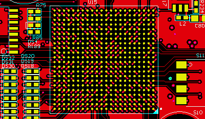
0.4mm-fine-pitch-BGA-PCB-Design-guideline

0.4mm fine pitch BGA PCB Design guideline

Nowadays, precise components is widely used in some advanced electronics devices, such as fine pitch FPGA component from Xilinx. But this take extra challenge to PCB designer and PCB manufacturing capability accordingly. Today, we simply discuss the PCB design guideline for 0.4mm fine pith BGA component to facilitate in PCB manufacturing. Standard guideline points: No … Continued

Most-common-stack-up-design-for-6-layer-printed-circuit-board

Standard 6 layer PCB stackup options

The standard 6L layers stackup is the most common options selected by most PCB designers. The standard layer stackup can be utilized in most applications. As a standard, you can get a variable layer stack up from Weller’s engineering suggestion, which is defined by following PCB thickness: 0.7mm/0.8mm/1.0mm/1.6mm/2.0mm/2.4mm/3.0mm Final finished copper thickness: 1/1/1/1/1/1oz ( (Note: … Continued

PCB-thermal-management-Copper-Coin-embeded

Embedded Copper coin and RFI Metal Backed PCB

Thermal management is very crucial in PCB design to transmit the heat of the PCB board with some critical high power components assembled. The four methods of thermal management 1. Thermal Vias,They can be mechanically drilled blind or through vias. 2. Laser, stacked micro-Vias, become more common, especially with low i/o pitch components. 3. Coppr … Continued

USB-connector-PCB-design

The stackup for 90 ohms impedance for USB

More and more PCB designers are interested in impedance track for USB circuit board of 90 ohm impedance. For 90 ohm impedance, there are two options of circuit track to get that: One option is to get 90ohm impedance by single-end impedance track, with stack up as below: The other option is by differential impedance … Continued

Printed-circuit-board-Design-and-Layout

Six Basic Principles of PCB Design

1. Principle One: Avoid Vias too Close to the SMT Pads If the via without oil plug hole, we will punch the via too close to the SMT pad during layout, which will cause the solder to flow through the via to the other side of the PCB during the reflow of the SMT pad … Continued

DFM services for PCB fabrication

Importance of Design Rule Check For PCB Manufacturing

The DRC (design rule check) is an in-depth review of your PCB fabrication data, which is carried out by our experienced CAM station engineers before production of your circuit boards even begins. The DRC is an extremely important step in circuit board manufacturing. The customer’s data are verified for manufacturability and for observance of required … Continued