1. Principle One: Avoid Vias too Close to the SMT Pads
If the via without oil plug hole, we will punch the via too close to the SMT pad during layout, which will cause the solder to flow through the via to the other side of the PCB during the reflow of the SMT pad , causing some problems such as insufficient SMT solder and then resulting in virtual soldering and etc. It is generally recommended that the distance between the edge of the via and SMT pads is more than 25 mils, and the via is covered with oil.

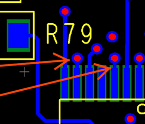
2. Principle Two: Do not Pull the Track Wider than the SMT Pad into the Pad Directly
If the track is larger than the pad, the window area of the SMT pad will generally expand more than the size of the pad, which causes the exposed copper part of the original SMT pad window to expand on the track, we make the opening of the Framed Stencil according to the size of the Pad, so it is better to wrap around . Anyway, it means that the amount of solder paste on the pad is slightly insufficient during Reflow Soldering, and there is a risk of virtual soldering. You will understand by looking at the picture below:
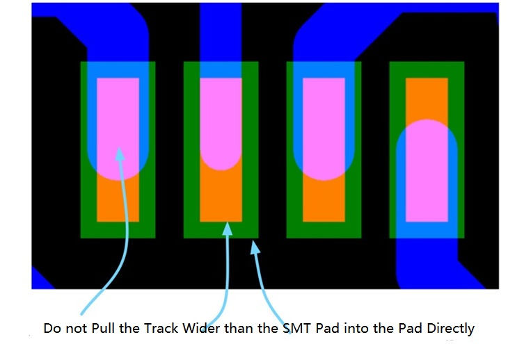
In addition, to use tracks larger than pads or slightly smaller than pads can also avoids the problem of excessive heat dissipation during Soldering.
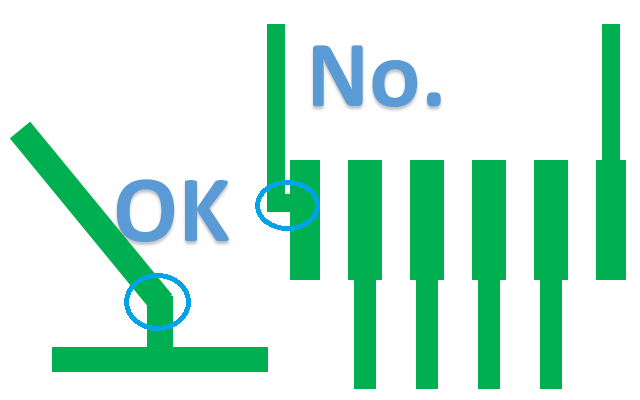
3. Principle Three: Do not Enter the Pad Parallel to the Edge of the SMT Pad When Routing
When you use small grids for wiring (grids <5mil), it is possible to pull the track into the pad which could parallel to the SMT pad side, and the distance between the track and the pad is very close (<5mil), please avoid this situation.Because this small U-slot will hide the corrosive potion, it will continue to corrode the cleaned PCB circuit, which will cause the hidden danger of virtual connection failure of the trace.
In addition, routing the wire into the pad in this way, as described in principle 2, will also make the SMT pad larger than the original design, causing hidden troubles in virtual soldering.

4. Principle Four: Avoid Routing at Acute Angles
Avoid routing at an acute angle in any case, even if it is a non-high-speed signal, because the acute-angle track will cause problems during the PCB manufacturing process. During the PCB circuit corrosion processing, the corner of acute angle will increase the corrosive effect PCB circuit corrosion is excessive, which will lead to the problem of open circuit.
As for high-frequency and high-speed circuits, it is necessary to avoid the use of acute angles. The track width at the corners is severely changed, causing impedance discontinuities and causing signal integrity problems.
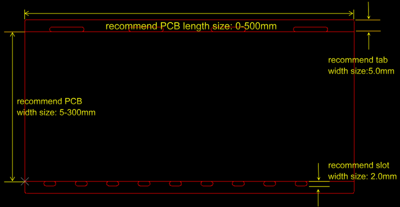
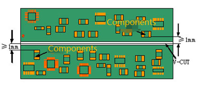
5. Principle Five: Do not Place Components too Close to the Edge of Board
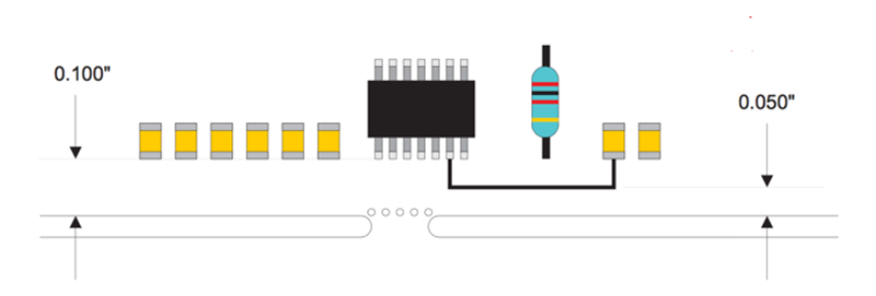
In the assembly and soldering phase of PCB, PCB will be transferred back and forth in various process areas, such as solder paste, transferred to the placement machine, and then transferred to the Reflow Soldering machine for soldering, so when we design PCB, there must be at least one pair of side on the board leave enough space on the opposite side for the conveyor belt, that is Breakaway Tab. The width of the Breakaway Tap is not less than 3mm, and the length needs to be not less than 50mm. There must be no interference between components and leads within the range of the Breakaway Tap, otherwise it will affect the normal transmission of the PCB board. If the layout of the PCB board cannot be satisfied, the method of adding a 3mm process edge or panel alone can be used. (Note: It is impossible to place SMT components within 5mm from the board edge on both sides of the Breakaway Tap, which is convenient for Reflow Soldering.) Of course, if the components on your PCB are manually soldered, you do not need to pass the conveyor belt, you can ignore.
If imposition is used, the components should be kept at a safe distance from the edge of the V-cut or stamp hole to avoid damage to the components or stress damage to the pads during board separation.
For PCB that require automatic board separation by the machine, both sides of the V-CUT line (Top and Bottom side) are required to retain device forbidden areas of each not less than 1 mm to avoid damage of the device during automatic board separation.
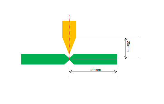
Meanwhile, it is also necessary to consider the structure of the blade of the automatic board splitter. Within the range of 5mm away from the boarding area of the board, it is not allowed to lay out devices with a height higher than 25mm.
When using V-CUT design, the above two items need to be considered comprehensively, whichever is more stringent. Ensure that the components will not be damaged during the V-CUT process, and it is convenient for PCB separation.
If the imposition is connected by a Stamp Hole, the components should be more than 100mil away from the edge of Stamp Hole plate.
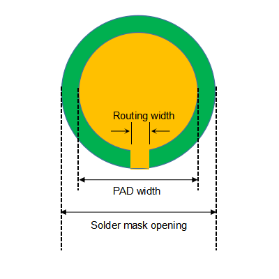
6. Principle Six: The Solder Mask Opening Window Needs a Uniform Size
We know that the PCB package pad needs to be Opening in Solder Mask. The Solder Mask Opening means that the pad area cannot be covered by green solder mask. In order to protect the PCB circuit from oxidation and short circuit during welding, our PCB outer layer is usually covered with a solder mask. The commonly used solder mask is green oil (certainly there are also black, red, yellow, blue, etc. oils).
But the pad can not be covered with green oil, so as to solder on the tin. In order to avoid solder mask on the pad due to process tolerances, which will affect the solderability of the pad, we generally design a larger solder mask opening area than the pad, generally expand 0.1 mm (4mil), of course, you can also not expand, so that the solder mask opening area is the same as the pad size, and the factory will handle it uniformly for you. But this requires when you are making the PCB package, the size of the solder mask opening must be the same, for example, they are as large as the pad size, or 0.1mm larger than the pad size.If there is some external expansion of 0.05mm and some external expansion of 0.1mm, it will be more difficult for the factory to handle.
Fore more information about PCB Design, warmly welcome to visit our website to get more details or contact us directly via [email protected].