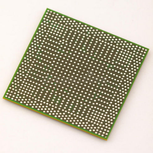
Nowadays, precise components is widely used in some advanced electronics devices, such as fine pitch FPGA component from Xilinx. But this take extra challenge to PCB designer and PCB manufacturing capability accordingly.
Today, we simply discuss the PCB design guideline for 0.4mm fine pith BGA component to facilitate in PCB manufacturing.
Standard guideline points:
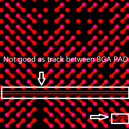
- No circuit track allowed between BGA PADs.
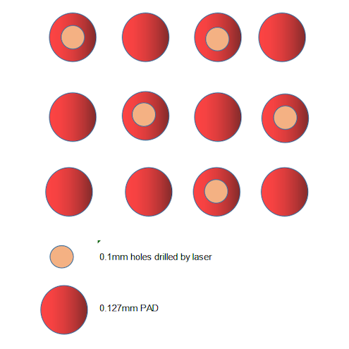
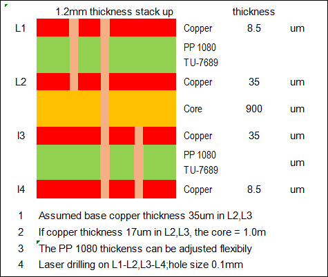
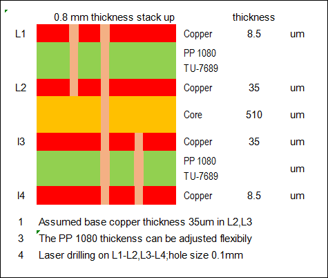
2. Minimum PAD size 0.127mm with 0.1mm laser hole drilled on (this could save space for PCB layout and reduce final PCB size). And suggest to use stack up: 0.8mm type or 1.2mm type.
3. The minimum spacing between track and holes:0.15mm(refer below picture)
4. Recommend to use Via in PAD design for BGA area holes.
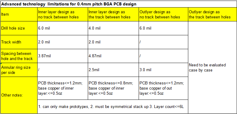
Advanced technology limitations for 0.4mm pitch BGA PCB design
Technology Map:
1.2mm stack up guideline (only for 4L):
0.8mm stack up guideline (only for 4L):
Important notes to surface treatment
Important notes to PCB surface treatment for 0.4mm fine pitch PCB:
| Surface finishing | Option |
| HAL(hot air solder leveling) | No-X(the surface is not so smooth so it will take trouble in soldering) |
| HAL Lead free | No-X(the surface is not so smooth so it will take trouble in soldering) |
| Immersion gold | Good-√ |
Important notes to PCB solder mask for 0.4mm fine pitch PCB:
| Solder mask Color | Option |
| Green | Good-√ |
| Black, red,yellow, white or other | No-X (difficult to keep solder mask dam) |
If you need stack up for 6L PCB board and have more questions to us please contact us by [email protected].