HDI (High Density Interconnect) PCB specified by it’s electrical holes structure, which is one of the fastest growing technologies in the PCB industry,it’s opposed type is through hole PCB.
In IPC-2226, it defines that HDI is a printed circuit board with a higher wiring density per unit area than conventional printed circuit boards (PCB).

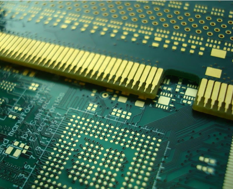
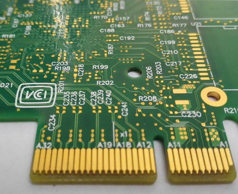
8L Gold finger BGA PCB 8L Gold finger HDI PCB
Compared to a conventional through hole PCB,the HDI PCB circuit board has a higher circuit track density,more finer circuit track width and spaces, minor via holes and capture pads, and much more higher connection pad density. And the HDI PCB boards often contain blind (drilling from top or bottom side to any mid-layer) and/or buried via holes (drilling from any mid-layer to any mid-layer side to any mid-layer) .Due to its minor hole size,drilling the smallest of micro-via hole is usually done by Laser Drill Technology.
PCB board designed by using HDI technology, circuit board designers would have the much more option to place more components on both sides of the board. It will release more I/O in smaller area as decreased component size and pitch benefit from HDI structures. This result in faster transmission of signals and will have a significant reduction in signal loss and crossing delays.
However, the placement of the component parts on a HDI circuit board require extra precision compared to a conservative PCB board design due to it’s miniature pads and fine pitch of the circuitry on the HDI PCB board.
Therefore, HDI technology can make reducing an 10 layer through-hole PCB to a 6 layer HDI micro-via PCB possible. The wiring capabilities of a well-designed 6 layer HDI PCB can achieve the same or even better functions than that of a standard 10 layer PCB.
Obviously that the micro-via process increases the cost of the board, but the proper design with reduction in layer count and material use reduces material cost accordingly, and many times would bring savings.
Main Types of HDI PCB Boards
- Through plated via holes from surface to surface,
- With buried and through via holes,
- More than HDI layers with through via holes,
- Passive substrate layers with no electrical connection,
- Coreless construction by layer pairs
- Alternative constructions of coreless constructions on layer pairs.
Highlighted Features HDI PCB
One outstanding feature of HDI PCB boards is that it’s track width/spacing can be designed as smallest as 3.0/3.0mil. These features help PCB designer to optimize the pad size significantly to release a much broader layout within each unit area.
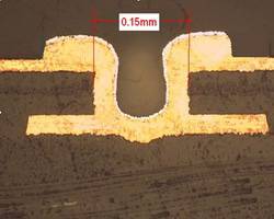
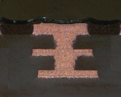
Another very super feature of HDI boards is its blind via holes, micro vias with it’s size can be optimized as 0.1mm, and it’s buried hole size can be optimized as 0.15mm. These features will greatly help PCB designer to be able to save space to populate more components on the limited area.
A blind via hole has similar characteristics with a through-hole via that at an internal point the board instead of passing through. But, a buried via only connects the internal layers of the PCB board, not including external layers.
These features enable the HDI PCBs have a higher circuitry density as compared to regular circuit PCBs.
HDI PCB Advantages
- Due to it’s high density circuitry, it enable HDI PCBs be able to be populated on both sides of the board to allow PCB designers to place more components onto smaller boards.
- Smaller size and lighter weight compared to through hole PCB
- Less layout count but high Electromagnetic Compatibility
- More convenience to PCB design and PCB layout work
- Good performance of impedance due to the less quantity of through plated holes.
- Less quantity of through plated hole, release more space for circuit track layout, improved EMI and RFI (ElectroMagnetic Interference / radio frequency Interference) due to the available shield plane.
- Can release more spaces for shield layer purpose to some critical components and tracks inside layer.
- Can release more spaces for some fine pitch components with BGA or QFN packages.
- Excellent performance of transmission and computing, apply to some high precision equipment such as smartphones, medical devices, as well as aerospace equipment.
Application of HDI PCB
• Digital communication
HDI technology supports more technology on fewer layers, as proving that bigger is not always better. Since the late 1980’s we have seen more and more consume electronic device such as camera, mobile phone, using cartridges the size of fitting in the palm of your hand. Mobile computing and working from our life pushed the technology further to make computers faster and lighter, enable the consumer to work remotely from anywhere
• Automotive
By saved spaces by smaller sized PCB, car manufacturers can have more space to place some smart interface for electronic device integrations in the care to provide more comfortable driving experiences for their customers, such as Tesla.
• Medical equipment
The diagnostic system and remote monitor system now is to come to common home due the technology drive the manufacturing possibility of it’s complex equipment
• Wearable technology
• Military and aerospace equipment
| Feature | WELLER´s technical specification |
|---|---|
| Number of layers | 4 – 24 layers standard, 30 layers advanced |
| Technology highlights | Multilayer PCB boards with a higher connection pad density than standard circuit boards, with finer lines/spaces, smaller via holes and capture pads allowing microvias to only penetrate select layers and also be placed in surface pads. |
| HDI builds | 1+N+1, 2+N+2, 3+N+3,4+N+4, any layer for prototypes |
| Materials | FR4 standard, FR4 high performance, Halogen free FR4, Rogers |
| Copper weights (finished) | 18μm(HOZ) – 70μm(2OZ) |
| Minimum track and gap | 0.075mm / 0.075mm(3.0mil/3.0mil) |
| PCB thickness | 0.40mm – 3.20mm |
| Maxmimum dimensions | 610mm x 450mm; dependant upon laser drilling machine |
| Surface finishes available | OSP, ENIG, Immersion tin, Immersion silver, Electrolytic gold, Gold fingers |
| Minimum mechanical drill | 0.15mm |
| Minimum laser drill | 0.10mm standard, 0.075mm advanced |
| Soldermask available | Green,matte green, black, matte black, white, blue, red,yellow |
Weller Technology is a professional in the field of (Printed Circuit Board) PCB assembly and manufacturing in China.We provide PCB fabrication service from a 2-50 layer, which includes HDI, Flex, Rigid, and Rigid-flex circuit boards. We also offer from low quantity to mass production, with high quality available at a reasonable cost.
With strong support behind you,we have experienced engineers in engineering as well as technician in production.We have experienced engineer So if you are looking to get the best and affordable HDI PCB manufacturing service, you will be rewarded by a supprise if you try it with us.