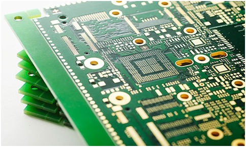
Nowadays the digital world is getting simpler and simpler. Your phone is getting smarter and your computer is no longer heavy.
You can work on your laptop and keep your business running while you board a flight. You can also watch your favorite action movie on your smartphone, or you can just plug in your wireless headphones and get into the groove. Mankind is fond of electronics and it has become a part of our lives. In this era, all the electronic devices are designed for portability. Electronic devices are being designed for human convenience. All this was possible because of the miniaturization of the components and PCBs inside the electronic devices.
As the size of the components shrunk smaller, printed circuit board manufacturers accommodated to the changing trend. This led to the birth of HDI PCB design.
What is HDI PCB?
HDI PCB is defined as a PCB with a higher wiring density per unit area than conventional PCB. They have finer traces and spaces, smaller vias and capture pads and higher connection pad density than employed in conventional PCB technology. HDI PCB is used to reduce size and weight, as well as to enhance electrical performance of the device. HDI PCB is made through Microvia and buried vias and sequential lamination with insulation materials and conductor wiring for higher density of routing. HDI PCB is the best alternative to high layer-count expensive standard laminate or sequentially laminated boards.
1. HDI Board Introduction
HDI PCB board is generally manufactured by the lamination method. The more the lamination times, the higher the technical grade of the board. Ordinary HDI boards are basically laminated one time, and high-level HDI circuit boards are laminated twice or more. At the same time, advanced PCB technologies such as hole stacking, plated hole filling, and laser direct drilling are used.
Electronic products are continuously developing towards high density and high precision. The so-called “high”, in addition to improving the performance of the machine, must also reduce the size of the machine. High-density integration (HDI) technology enables smaller end product designs while meeting higher standards for electronic performance and efficiency. At present, many popular electronic products, such as mobile phones, digital cameras, notebook computers, automotive electronics, etc., use HDI circuit boards. With the replacement of electronic products and market demand, the development of HDI circuit boards will be very rapid.
2. Are PCB boards with blind and buried holes called HDI boards?
HDI PCB boards are high-density interconnection circuit boards. The boards with blind hole plating and secondary lamination are HDI boards. They are divided into first-stage, second-stage, third-stage, fourth-stage, and fifth-stage HDI, etc. For example, the mother board of iPhone 6 is fifth- stage HDI.
The simple buried hole is not necessarily HDI board.
3. The difference between HDI board and conventional PCB
Conventional PCB board material is mainly FR-4, which is made of epoxy resin and electronic grade glass cloth. Generally, conventional HDI uses adhesive-backed copper foil on the outermost side. Because laser drilling cannot penetrate glass cloth, it is generally necessary to use adhesive-free copper foil without glass fiber. However, high-energy laser drills can already penetrate 1180 glass cloth.. This is no different from ordinary materials.
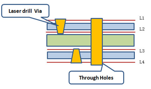
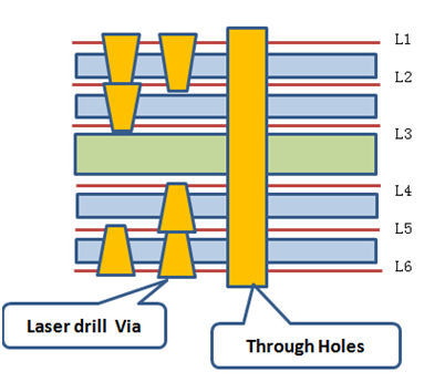
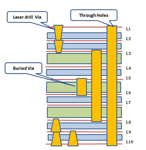
4. The different types of HDI PCB stack-ups
- 1+N+1 – PCBs contain 1 build-up of high-density interconnection layers.
- i+N+i (i≥2) – PCBs contain 2 or more build-up of high-density interconnection layers. Microvias on different layers can be staggered or stacked
- i+bN+i (i≥2)- includes buried vias
- Any layer HDI – All the layers of a PCB are high-density interconnection layers. This allows the conductors on any layer of the PCB to be interconnected freely with copper filled stacked microvia structures.
What are the advantages of HDI PCB?
Generally HDI circuit boards have the following advantages:
- Reduce the PCB cost: When the density of PCB increases by more than eight layers, it will be manufactured by HDI, and its cost will be lower than the traditional complicated lamination process.
- Increase circuit density: The interconnection of traditional circuit boards and parts must be connected through the lines and via-hole conductors drawn out around the QFP (fan-in and fan-out), so these circuits need to occupy some space. The microvia technology can hide the wiring required for interconnection to the next layer. The connection between the pads and the leads between different levels is directly connected by the blind holes in the pads, without the need for fan-in and fan-out wiring. Therefore, some pads (such as mini-BGA or CSP small ball bonding) can be placed on the outer layer board to accept more parts, which can increase the density of the circuit board. Many high-function small-sized wireless phone handset boards use this new stacking and wiring method.
- Conducive to the use of advanced assembly technology: Generally, the traditional drilling technology cannot meet the needs of small parts of the new generation of thin circuits due to the size of the pad (through hole) and mechanical drilling. With the advancement of microvia technology, designers can design the latest high-density IC packaging technology, such as Array package, CSP and DCA (Direct Chip Attach), into the system.
- Better electrical performance and signal accuracy: The use of micro-hole interconnects can reduce signal reflection and cross-talk interference between circuits, and allow more space for the circuit board design. Due to the physical structure of the micro-holes The nature is that the holes are small and short, so the effects of inductance and capacitance can be reduced, and the switching noise during signal transmission can also be reduced.
- Higher reliability: Due to the thinner thickness and 1: 1 aspect ratio of the micro-holes, the reliability of signal transmission is higher than that of ordinary through-holes.
- Improved thermal properties: The insulating dielectric material of HDI boards has a higher glass transition temperature (Tg), so it has better thermal properties.
- Improve radio frequency interference/ electromagnetic wave interference/electrostatic discharge (RFI/ EMI/ ESD): micro via technology can allow circuit board designers to shorten the distance between the ground layer and the signal layer to reduce radio frequency interference and electromagnetic wave interference; on the other hand, the number of ground wires can be increased to avoid damage to the parts of the circuit due to the instantaneous discharge caused by static electricity accumulation.
- Increase design efficiency: The micro via technology allows the circuit to be arranged on the inner layer, so that the circuit designer has more design space, so the efficiency in circuit design can be higher.
For more information about HDI PCB or HDI PCB manufacturing capabilities, please visit https://pcbweller.com/hdi-pcb-capability/ or directly contact us by email.