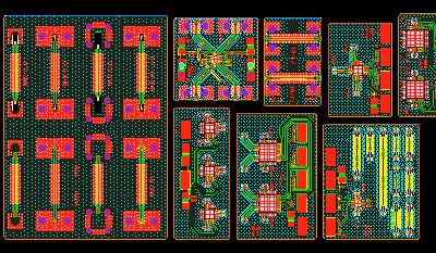
PCB panel design and manufacturing

How to design couple of different PCBs in one panel

Optimize the global manufacturing cost of PCB and PCBA prototypes When it comes to start a PCB design for prototypes, Most circuit board designers like to put various PCBs (the same layer count and stack up but with difference in size, shape etc) into one panel to optimize the cost in the PCB fabrication and … Continued

Encapsulation and PCB Assembly Potting Services

Two options of potting epoxy resin to PCB assembly devices.

WellerPCB as a China Printed Circuit Board manufacturer and your offshore PCB Manufacturer has several years of experience successfully manufacturing PCB’s that are RoHS compliant and are compliant with lead-free assembly. We offer a variety of laminate and surface finish options.

controlled-impedance-PCB-manufacturer

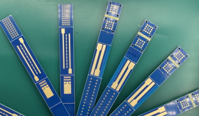
What is the PCB impedance coupons

The brief summary about PCB impedance PCB board with controlled impedance trace is very important for signal transmission quality.Especially for quick switching parts with signal rise times of 1 to 2ns, the signal integrity must be guaranteed through good impedance characteristics in the conductor trace connections. What is the PCB impedance coupons The PCB impedance … Continued

16-layers-pcb-manufacturer

Standard 16 layer PCB stackup options

Our standard 16L layers stackup is the most common options selected by most PCB designers. The standard 16 layer stackup can be utilized in most applications for multilayer PCB board. As the standard options, you can get a variable 16 layer stack up from Weller’s engineering suggestion, which is defined by following with 3 options … Continued

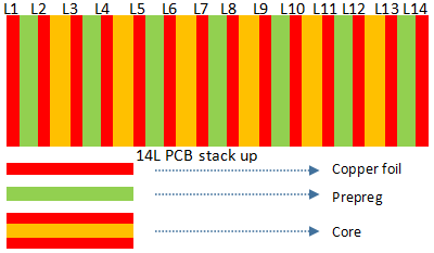
14L-rigid-PCB-stack-up-design

Standard 14 layer PCB stackup options

Our standard 14L layers stackup is the most common options selected by most PCB designers. The standard 14 layer stackup can be utilized in most applications for multilayer PCB board. As the standard options, you can get a variable 14 layer stack up from Weller’s engineering suggestion, which is defined by following with 3 options … Continued

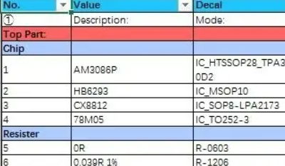
Bill of Materials for PCB assembly

How to create an effective PCB assembly BOM file

BOM file is one of necessary documents for PCB board assembly process, except other documents like PCB Gerber file, Pick and Place file, silkscreen file. For PCB designer, it is very important to create an effective BOM file to save time for PCB assembly house to make correct quotation for components and improve efficiency in … Continued

12-layer-pcb-manufacturer

Standard 12 layer PCB stackup options

Our standard 12L layers stackup is the most common options selected by most PCB designers. The standard 12 layer stackup can be utilized in most applications for multilayer PCB board. As a standard option, you can get a variable 12 layer stack up from Weller’s engineering suggestion, which is defined by following : PCB thickness: … Continued

10-layer-pcb-manufacturer

Standard 10 layer PCB stackup options

Our standard 10L layers stackup is the most common option selected by most PCB designers. The standard layer stackup can be utilized in most applications. As a standard, you can get a variable 10 layer stack up from Weller’s engineering suggestion, which is defined by following : PCB thickness: 1.3mm/1.6mm/2.0mm/2.4mm/3.0mm Final finished copper thickness: 1/1/1/1/1//1/1/1/1/1oz … Continued

8-Layer-rigid-pcb-stack-up

Standard 8 layer PCB stackup options

Our standard 8L layers stackup is the most common option selected by most PCB designers. The standard layer stackup can be utilized in most applications. As a standard, you can get a variable 8 layer stack up from Weller’s engineering suggestion, which is defined by following : PCB thickness: 1.0mm/1.6mm/2.0mm/2.4mm/3.0mm Final finished copper thickness: 1/1/1/1/1//1/1/1oz … Continued