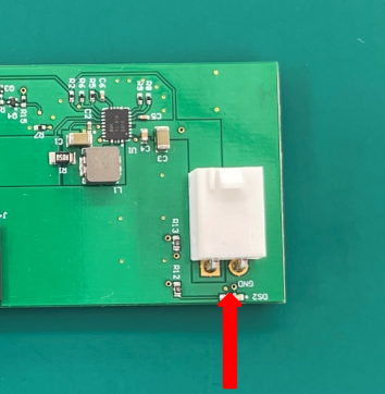
Within any simple electronic devices we used nowadays, there is a PCB (printed circuit board) drive it to run. The PCB is the core component of the electronic devices, whether it is a consume product such as battery charger, the communication equipment such as mobile phone, or transportation tool such as vehicle, even it is a complicated industry control system such as embedded computer. Simply thinking that is composed by a series of components and resistors, but actually it is so not.
The PCB assembly is to have necessary electronic components to be purposely assembled on the bare printed circuit board(PCB), the process critical to get right the first time. Any single mistake in this work could result in malfunctions, or even some unexpected accidents. In this article, we’ll simply present some critical PCB assembly process steps and something what you should know.
It’s Not PCB board manufacturing
It is not a manufacturing process; more or less it can be understood as “composed” work. PCB manufacturing is to generate the physical PCB board from different raw materials by specific manufacturing process.
But PCB assembly process takes place during a specific time in the development of an integrity electronic device. So it’s not about manufacturing. Thus, at WellePCB, we’ll manufacture the bare PCB board itself, including all the prototypes or mass productions, and then work on PCB assembly.
In a word, PCB assembly is the process of that taking necessary material (including PCB board) together into one place and compose them by specific time and steps. And then making sure it well works as what it is intended to do.
How to Thoroughly Understand the PCB Assembly Technologies
To correctly assemble a PCB board requires Not only just the raw electronic components and a well-manufactured PCB board. It also requires the right technology and advanced equipment machines. In this case, there are several options needed to be considered, and each generate something different to the result.
For example, there’s some regular soldering process such as surface mount technology (SMT), wave peak soldering, manual soldering, as well as selective soldering wave peak soldering.
While some common PCB assembly processes will require just one type of technology, but others will require a complex combination of two or more technologies. For example, many PCB boards require the combination of through-hole technology (THT) and surface mount technology (SMT). Therefore, well understanding when, where, and how to integrate those technologies is a critical consideration before officially choosing a PCB Assembly company to handle your project or production.
It’s also important to understand that the basic PCB assembly steps should be involved with the various technologies differ, too. Below, we’ve outlined some basic steps involved, as well as how they differ from technology to technology.
An Overview To PCB Assembly Process
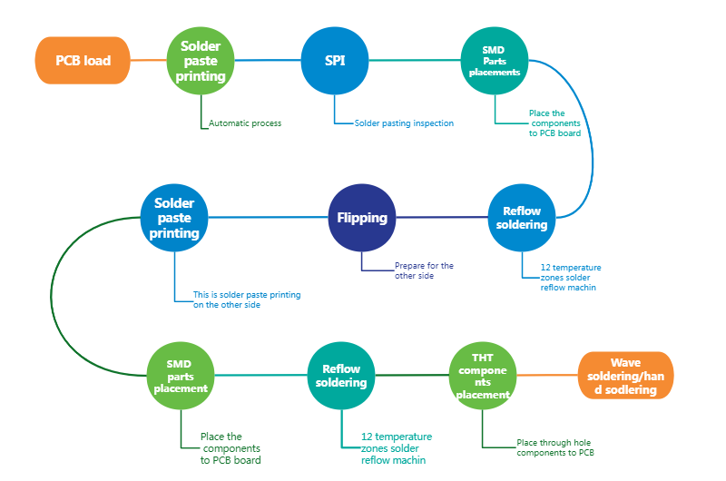
Solder Paste: This is the first step of a PCB assembly process. But note that this is not the case with THT process, but SMT process does require paste application and/or printing. This is normally done by auto-machine, some of manufacturer is still using manual-working printing which have unstable quality to next step of components placement.
Components Placement: This is next the step in PCB assembly process that to place the electronic component (SMD components such as resistors,capacitors,etc ) on the the PCB board by an automatic SMT machine.Of course,this can be done manually, but it’s not a good option due to it’s unstable quality. In THT assembly, components are mostly placed by hand, which requires high precision. In the SMT process, it is to use robotic systems to place the components on the bare PCB board. Reasonably that automated placement is far faster than manual placement and is just as precise.
Soldering Reflow: In the regular PCB assembly process, the next step is soldering reflow, which is when the printed solder is first melted and then re-solidified. The PCB board and all its electronic components move through an oven, which heats the solder by high temperature, liquifying it and ensuring that connections between components and PCB board are formed before the circuit board moves into a cooler zone, where the solder is to be cooled.
However, we need to know that the THT process does not require re-flowing solder. Instead of that, the second step here is to inspect the assembled PCB board and rectify it’s component placement. This is due to the manual placement process – a visual inspection in conjunction with a design transport frame helps ensure placement accuracy.
In the SMT process, reflow soldering takes place at this time, as well. The circuit board with components placed on is sent through a tunnel furnace, which heats and melts the solder paste, allowing it to flow as necessary, before the board passes through a series of coolers that gradually operate the temperature down, solidifying the solder on the PCB board and the components are electrically secured to the printed circuit board.
Inspection: The next step in the traditional PCB assembly process is a visual inspection to assembled PCB board, soldering, and components. This is process normally performed by automatic machine (AOI),which have secured precision;or by manual work (just for some simple assembly and prototypes). Note that this step has already occurred in the both THT and SMT processes.
Through-Hole Components Assembly: The traditional process to do through-hole components insertion by manual work, after the reflow soldering and inspection process. It’s soldering is also often done manually, but it may be done by using wave peak soldering or selective wave soldering(depends on your requirements and design on through hole component).
Wave soldering occurs during the THT process at this point, as well. By the process that the printed circuit boards to be soldered over a wave of solder.
By this way a complete electronic PCB board can be soldered in a matter of seconds producing joints that are reliable mechanically and electrically.
Final Inspection and Cleaning: The last step in the traditional circuit board assembly process is a final inspection of the assembled PCB board upon some inspection standard criteria such as IPC-A-610, the solder points, and the electronic components, and a cleaning to ensure that debris or excess solder is removed.
What IS The Right PCB Assembly Process For You
Although the SMT assembly process is faster and often more precision than either the traditional PCB assembly process or the THT process,however, it is not always the best option. For example, if you only need a very simple prototype board assembled, the THT process might be the better choice. Each situation differs and there is no single solution that will always work for every need.
Weller is a PCB Assembly Company with more than 10 years of experience, we well understand that customer’s needs, budgets, and goals vary. We pride ourselves on offering exactly and the professional solutions that each customer needs.
Whether you’re producing a simple prototype for proof of concept purpose or you’re ready to move it into a formal production with thousands of units being produced, we can help.
Contact us freely to present your consultation or to know more about our assembly services and capabilities.