This is second electrolytic plating stage that to electrically plates copper onto the exposed metal surfaces ( in areas without dry film (circuitry)).
By this process,the copper will be plated up to a thickness with and average of 25um / min 20um through the hole. Once the copper has been plated, tin is applied to protect the plated copper(which will be il).

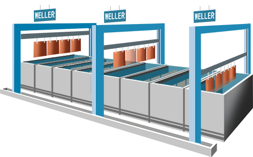
WELLER’s standard copper thickness of through hole is 25um (nominal), which equates to IPC class 3,this thickness can provide much more greater reliability of the via structure and improved z-axis expansion performance.
3 basic steps in pattern plate process: