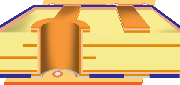
This is simply a three step process.
![](https://pcbweller.com/app/uploads/2020/11/PCB-outlayer-etching-process.png)
The first step is to remove the blue dry film to expose the unwanted copper.
![](https://pcbweller.com/app/uploads/2019/08/pil_ned.png)
![](https://pcbweller.com/app/uploads/2020/11/PCB-outlayer-Resist-Strip.png)
The second step is to etch away the exposed/unwanted copper but now the tin deposit acts an etch resist protecting the wanted copper.
![](https://pcbweller.com/app/uploads/2019/08/pil_ned.png)
![](https://pcbweller.com/app/uploads/2020/11/PCB-outlayer-etching-before-tin-strip.png)
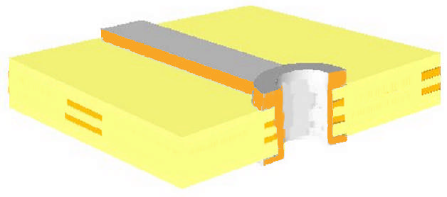
The third and final step is to chemically remove the tin deposit leaving the pads and traces on the panel surface.
![](https://pcbweller.com/app/uploads/2019/08/pil_ned.png)
![](https://pcbweller.com/app/uploads/2020/11/PCB-outer-layer-Tin-Strip.png)
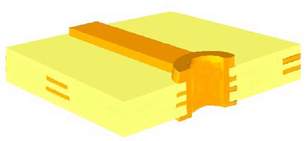
Then the tin is chemically removed leaving behind a bare copper and laminate panel. The surface pads, traces and plated through holes are the exposed copper. This is the last step in strip-etch-strip.
![](https://pcbweller.com/app/uploads/2019/08/pil_ned.png)
![](https://pcbweller.com/app/uploads/2020/11/pcb-outlayer-etching-process-final-step.png)
![](https://pcbweller.com/app/uploads/2019/08/pil_ned.png)
![](https://pcbweller.com/app/uploads/2020/11/PCB-outer-layer-etch.png)