The similar process as the inner layer’s (perform the image transfer by using photosensitive dry film, exposure to UV light and etching).Only with one main difference:the dry film where we want to keep the copper/circuit track will be removed– so as that we can plate additional copper later in the process.
This step of the process is performed in a high grade clean room.
The detail of steps of outlayer imagine process is as below:
Dry-film Resist Coating Outer Layer Panels
The same resist or light sensitive film used on the inner layers is used for the outer layers. The film covers the entire surface including the drilled holes.

Outer Layer Expose & Develop
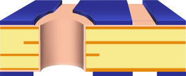
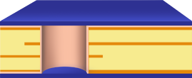
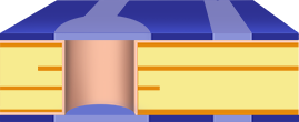
After dry film lamination the panel is exposed and developed using the same procedure used for the inner layer cores. Clear areas in the film allow light to pass through and harden the resist creating an image of the circuit pattern All of the drilled holes that are exposed will be plated through.
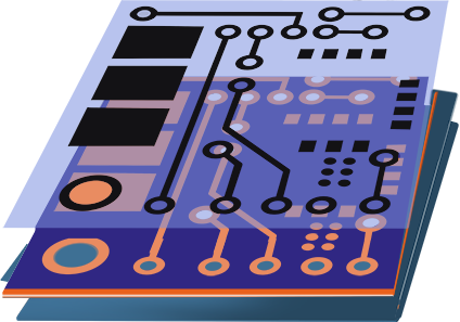
Copper “Pattern”Plate
The electroplating processes that electrically plates copper onto the exposed metal surfaces is next. The copper will be plated up to a thickness of approximately 1 mil (0.001”), depending on the required final finish for the panel.