This is to remove the unwanted copper from the working panel by using chemical etching.
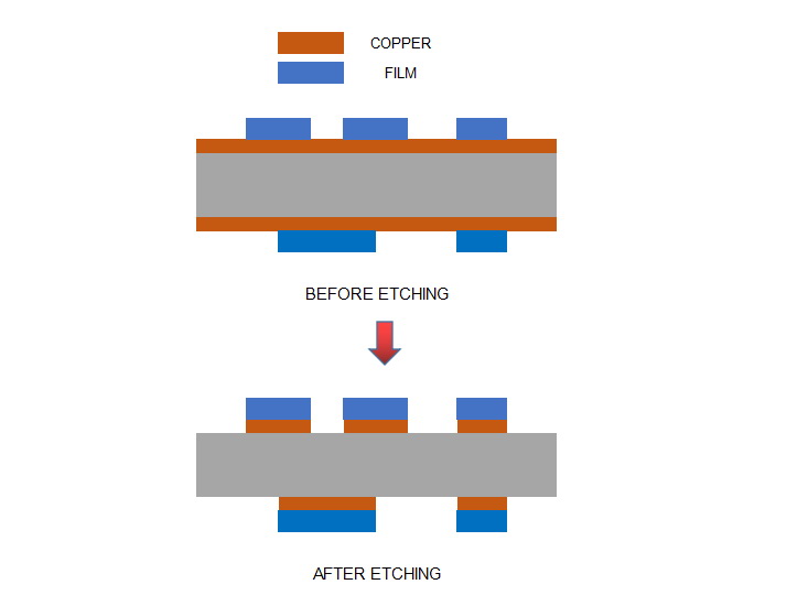
After the unwanted copper has been removed, the remaining dry film is then to be removed off and leaving behind the copper circuitry that matches the circuit design.
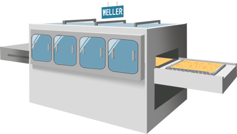
WELLER’s Value:
Advanced automatic control etching production line with high deficiency work from start to end without any manual process.