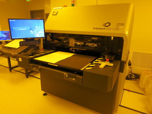
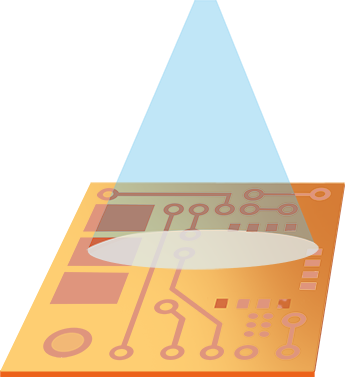
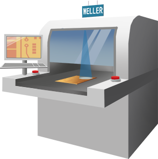
Through scanning of the production circuit board to catch out the defects via comparing the exist circuit against the digital “images” from original design.
The purpose of this stage is to sort out the defects PCB in inner layers production, and do not leave it to next production process.
WELLE’s value:
Latest leading AOI machine+90% automatic running instead of manual scanning work.