1. The preface of copper coin embedded PCB
Today in electronics industry filed, The power of the electronics is more and more higher than before, but the body size of the product is much smaller accordingly, which is a huge challenge to electronics.
Copper coin embedded PCB is a popular design of solution to high heat dissipation’s electronics product.
2. The types of copper coin embedded PCB
The two common types design of copper coin embedded PCB:
- copper coin thoroughly embedded
- copper coin buiried embedded
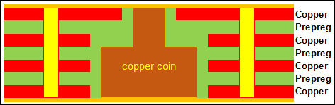
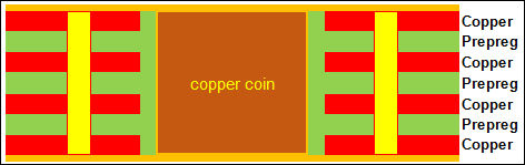
2-1. Copper coin thoroughly embedded type
The thickness of copper coin is same as the PCB thickness,two types of copper coin:
- Un-stacked copper coin,
- And stacked copper cion

stacked copper coin through copper coin
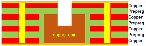
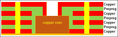
2-2. Copper coin buried type
The thickness of the copper coin is thinner than PCB board thickness, there is routing window the PCB board;two types of copper coin:
- Cavity rouing slot on the copper coin,
- No cavity routing slot on the copper coin
cavity copper coin no cavity copper coin
3. The key points and action process of production on Copper coin embedded PCB
See below table for key points of production design for copper coin embedded PCB
| Item | Key points | Control action |
| 1 | The stickness between copper coin and PCB board | A. stack up:consist of multi-prepreg 1080,make sure the resin filling fully. B. Need high Tg base material C. treament the copper coin with Black oxide or brown oxide |
| 2 | the flatness between copper coin and PCB board: +/-50um. | A. the theoretical thickness of copper coin should be same as PCB board thickness. B. the tickness tolerance of copper coin +/-0.025mm C. before laminate press, need copper foil and aluminum foil match-work to generate cushion. |
| 3 | The match features between copper coin and cavity routing from the core(prepreg) | A. The size of cavity routing in inner core should be larger than copper coin 0.1mm per side. B. The size of cavity routing in inner prepreg should be larger than copper coin 0.2mm per side. C. the tolerance of copper coin’s dimensions:+/-0.05mm D. Process of cavity on the core and prepreg: pre-routing+accurate routing,control the tolerance of routing cavity :+/-0.1mm |
| 4 | The drilling of belind holes and the cavity routing on the copper coin after copper coin embedded | A. Blind hole size on the copper coin: >=0.10MM,and keep the Aspect Ratio of blind holes >1 B. Cavity routing need t o be produced by special CNC tooling,and keep the high flatness of cavity. |
4. The preface of production design
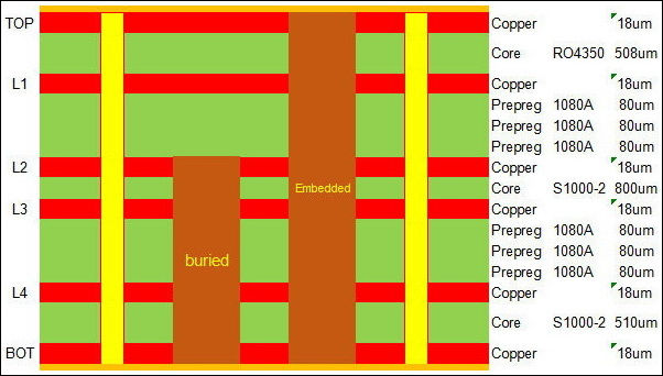
4-1. The stack up design-refer below stackup details
Brown color is the copper coin; 3 PCS of 1080 prepreg filled between L1-L2,L3-L6,to make sure the spacing (copper coin and PCB body) to be fully filled by resin of prepreg.
4-2. The production process
(1). The process of Prepreg: Laminate cutting->laminate pressing->drill holes->inspecting->accessory material matching.
(2). Aluminum foil process: Laminate cutting>accessory material matching.
(3). The process of inner core: Laminate cutting->inner image transfer->inner etching inspection->inner layer fixing hole->plating hole(need CCD machine to drill 4 PCS of fixing hole)->laminate material matching->black oxide treatment
(4). The process of copper coin: copper coin manufacturing(subcontractor)->black oxide treatment
(5). The top-bottom layer process: Laminate press->polishing->PTH(1)(do not do desmear process )->copper plating->drill holes->back drilling(drilling the blind holes by depth-controlled drilling machine )->routing the cavity holes(use special CNC machine to route the cavity )->copper into hole–>outlayer image->plate Sn-copper->outlayer etching->solder mask->the following regularly process.
Special notes to laminate stack up process:back orientation of top side circuit track layer, with putting 1oz copper foil under the layer. But an aluminum foil on bottom side layer, following next step of regular stack up process.
4-3: The key design points of design
| Item | Key control process | Design scheme |
| 1 | the thickness of the copper coin and PCB core;and the match features of cavity routing | (1) the PP routing cavity window and the core where the copper coin embedded: the outing cavity size on the core should be larger than copper coin as 4mil per side; the routing cavity size on the PP should be larger than copper coin as 8mil per side (2) the cavity routing hole on the core and PP manufacturing by the method of pre-routing + formal routing, the formal router tooling size 1.0mm, the tolerance of cavity routing hole size +/-0.10mm (3) thickness of through-type-copper coin: 2.30mm; the thickness of buried copper coin 1.50mm,need to radius corner treatment size R=1.0mm to copper coin. See below picture: the outlayer profile is the routing path of core,and the inner profile is the profile of copper coin, the 4 corners on both profiles need to be treat as R=1.0mm  |
| 2 | The copper coin treatment:black oxiden+brown oxiden | Use customed fixture tooling for copper coin to start production, fixture tooling made of FR4 material with 3.0mm thickness. There are 3 types size of blind cavity(apply for different kinds of blind cavity),to drill 2.0mm through holes on the blind cavity routing (for the purpose of the flow of chemical potion). The illustration of fixture tooling. |
5. Conclusion:
Follow above steps and key points of production process and the normal PCB manufacturing process, the copper coin embedded PCB successfully manufacturing out. See below table for details:
5-1. The quality overview on the copper coin embedded PCB
| The overview of copper coin embedded zone | the detail review of copper coin embedded zone |
| The temperature of samples production: 288+/-5℃ with merging into the Pb-Sn tank for 10 seconds, thermal stress test 3 times; no delaminating, no blister; PASS. | Test 3 times by lead-free reflow soldering process, no delaminating, no blister, PASS. |
5-2. The micore section of flatness of PCB copper coin embedded zone.
| Analysis the flatness of copper coin with it’s PCB surface,the copper coin is smooth and fat,the difference of height is 13.8um,Accept. |
 |
For more concerning about copper coin embedded PCB design and production,please let us know freely by [email protected]