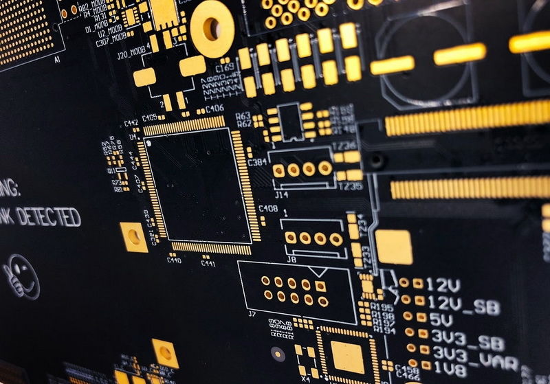
PCB Prototype is a critical stage in the electrical product development. It enables to eliminate the flaws in design and avoid it taken to mass production to the reduce the risk of costly rework during mass production.
At Weller Technology, a variety of different kinds of printed circuit board prototypes can be manufactured according to your specifications, no matter it is single or double-sided PCB, blind or buried via boards, heavy copper PCB boards, metal-back PCBs, high frequency PCB made with unique materials or rigid-flex PCB and rigid PCB with burn-in board testing. Weller Technology can take your design idea to fruition.

We have PCB prototype fabrication technology capability as multilayer PCB over 50 layers with quickest lead time within 24 hours for 4L board. Plus our PCB assembly capacity of 7 STM lines, 2 DIP production lines and electronic functional test, Weller can support you one-stop service for PCB prototype fabrication and assembly.
Weller Technology even can also provide DFM (Design for manufacturing) service for prototype PCB manufacturing. Our experienced engineers will provide PCB designer with an optimized blueprint along with their design process, which will eliminate the possible manufacturing problems from beginning of the project. Instead of other manufacturer’s blind following up customer to directly manufacture, Weller Technology can have your projects at right design and manufacturing at the first time.
No matter that you choose our PCB prototype manufacturing service with DFM support or use your own design instead, all of the requirement and specification will be double reviewed and evaluated by our experienced engineer and it’s circuit boards will be tested to ensure it can be applied and expectedly work in your projects.
PCB Prototype Advantages
- All potential design flaws can be detected out from the beginning of your project. This can save your time and money before the flaws result in extra rework or projects failure costs once direct mass production.
- With less cost-spending when compared with the mass-volume production orders, prototype work will give you a clear blueprint that how small tolerance and strict quality can be controlled, and sometimes it even can explore some unexpected issues. Anyway, it’s a valuable step to ensure the perfection of further standard PCB production.
- From the test of assembled prototypes PCB,PCB designer can detect and correct the bugs in software and modify the design of the hardware to make them compatible with each other
How to Order and Track Your Prototype PCB
At any time, you can contact us freely by providing your design on PCB Gerber files, along with a full BOM list; our skilled engineers will double evaluate the design and offer you the quotation along with our DFM report.
We absolutely know the lead time of critical is very important, so your prototypes orders will be carefully monitored every day by our sales team until it successfully delivered to your hand by express service.
PCB Prototype Manufacturing Capability from Weller Technology
| Feature | Weller´s technical specification |
|---|---|
| Number of layers | 4 – 22 layers standard, 30 layers advanced, 40 layers prototype. |
| Technology highlights | Multiple layers of epoxy glass fiber bonded together with multiple layers of copper of varying thicknesses. |
| Materials | High performance FR4, halogen-free FR4, low loss and low Dk materials |
| Copper weights (finished) | 18μm – 210μm, advanced 280μm / 8oz |
| Minimum track and gap | 0.075mm / 0.075mm |
| PCB thickness | 0.40mm – 7.0mm |
| Maxmimum dimensions | 580mm x 1080mm, advanced 610mm x 1400mm |
| Surface finishes available | HASL (SnPb), LF HASL (SnNiCu), OSP, ENIG, Immersion Tin, Immersion Silver, Electrolytic gold, Gold fingers |
| Minimum mechanical drill | 0.15mm |
| Hole Tolerance | PTH: ±0.075, NTPH: ±0.05 |
| Solder Mask Color | Green/Black/White/Red/Blue/Yellow |
| Silkscreen Color | White, Blue, Black, Red, Yellow |
| Min Annular Ring | 3.0mil |
| Board Thickness Tolerance | ±0.1mm – ±10% |
| Board Size Tolerance | ±0.1mm – ±0.3mm |
| Copper Thickness Tolerance | +0μm +20μm |
| Inner Layer Copper Weight | 0.5oz – 3.0oz |
| Hole Plating Thickness | 20μm – 30μm |
| Plated Hole Size Tolerance | PTH: ±0.075 |
| Non-Plated Hole Size Tolerance | NTPH: ±0.05 |
| Aspect Ratio | 1:10 (Hole size: Board thickness) |
| PCB Eelctrical Testing | 10V – 250V, flying probe, Or testing fixture |
| Impedance Tolerance | ±5% – ±10% |
| SMD Pitch | 0.2mm (8mil) |
| BGA Pitch | 0.2mm (8mil) |
| Chamfer of Gold Fingers | 20, 30, 45, 60 |
| Solder Mask Bridge | 0.1mm |
| Minimum distance between plated holes and trace | >=12 mil |
| Minimum distance between plated holes and trace | >=12 mil |
| HDI builds | 1+N+1, 2+N+2, 3+N+3,4+N+4, any layer in R&D |
| Minimum laser drill | 0.10mm standard, 0.075mm advanced |
| Back-drill | Available |
| Depth-control drill | Available |
| Copper coin embedded | Available |
| Resistors embedded | Available |
| IPC Criteria | class 2, class 3 |
| MOQ | 1PCS |