Coplanar Waveguide is a type of PCB Impedance
When it come to talk about PCB impedance, often it refer to talk single-end impedance,differential impedance.
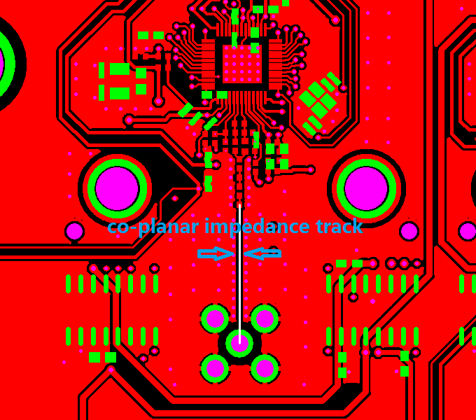
There is another type of impedance called co-planar impedance.
What is co-planar impedance
It is the impedance measured from signal track when it transmit the signals between GND and VCC zone.
What is coplanar gaveguide circuits
Co-planar (also called Coplanar waveguide) track is a type of electrical planar transmission line which can be fabricated using printed circuit board technology, and is used to convey microwave-frequency signals.
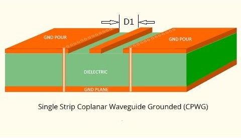
Basically, a coplanar waveguide (CPW) consists of a conductor separated from two ground planes, and everything is etched on one side of a dielectric on the same plane. The dielectric should be thick enough to damp the electromagnetic fields inside the substrate.
Coplanar waveguide impedance model in Polar Si9000
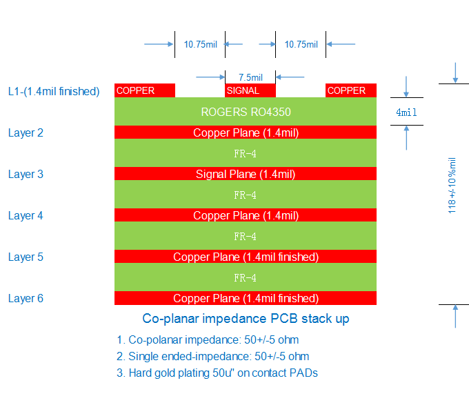
In Polar impedance model, comparison with single ended impedance and differential impedance model, coplanar impedacne has 1 extra feature of “D1” . D1 means the spacing that the impedance track keeping from it’s reference layer VCC/GND.
In polar Si9000,there are 4 models for coplanar waveguide impedance calculation,which highlighted in red in below configuration.
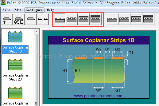
Point at the impedance model of coplanar waveguie,we just take some typical model from Polar SI9000 to make a summary presentation.
Please note these models is typical of waveguide.
- Surface coplanar waveguide 1B
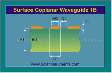
Application: Single coplanar waveguide track after etching in out layers, the track surrounded by VCC/GND which is shield reference “layer”, and the following layer (innerlayer 2) is single track layer, not VCC/GND shield reference layer.
Presentation:
| H1 | The dielectric thickness between outlayer and it’s following layer(inner layer 1) |
| W2 | The upper width of the impedance track(refer above configuration) |
| W1 | The bottom width of the impedance track(refer above configuration) |
| D1 | The spacing of impedance track to it’s VCC/GND zone(in the same layer) |
| T1 | Thickness of impedance track=base copper thickness+plating copper thickness |
| Er1 | Dielectric value of core or prepreg |
2. Coated coplanar waveguide 1B
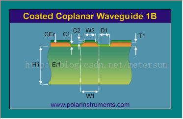
Application: Single coplanar waveguide track after solder mask, the track surrounded by VCC/GND which is shield reference “layer”, and the following layer (innerlayer 2) is single track layer, not VCC/GND shield reference layer.
Presentation:
| H1 | The dielectric thickness between outlayer and it’s following layer(inner layer 1) |
| W2 | The upper width of the impedance track(refer above configuration) |
| W1 | The bottom width of the impedance track(refer above configuration |
| D1 | The spacing of impedance track to it’s VCC/GND zone(in the same layer) |
| T1 | Thickness of impedance track=base copper thickness+plating copper thickness |
| Er1 | Dielectric value of core or prepreg |
| CEr1 | Dielectric value of solder mask |
| C1 | the solder maks thickness on laminate |
| C2 | the solder mask thickness on copper track |
3. Surface coplanar waveguide with ground 1B
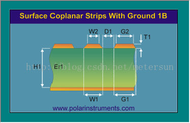
Application: Single coplanar waveguide track after etching in out layers, the track surrounded by VCC/GND which is shield reference “layer”, and the following layer (innerlayer 2) is single track layer, not VCC/GND shield reference layer.
Presentation:
| H1 | The dielectric thickness between outlayer and it’s following layer(inner layer 1:VCC/GND Zone) |
| W2 | The upper width of the impedance track(refer above configuration) |
| W1 | The bottom width of the impedance track(refer above configuration |
| D1 | The spacing of impedance track to it’s VCC/GND zone(in the same layer) |
| T1 | Thickness of impedance track=base copper thickness+plating copper thickness |
| Er1 | Dielectric value of core or prepreg |
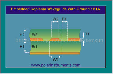
4. Edge-coupled Offset stripline 1B1A
Application: Single coplanar waveguide track in inner layers, the impedance track surrounded by VCC/GND zone, the next inner layer 2 is track layer. not reference layer of VCC/GND.
Presentation:
| H1 | The dielectric thickness between impedance trak layer and it’s following layer(inner layer 1:VCC/GND Zone) |
| H2 | The dielectric thickness between impedance trak layer and it’s following layer(inner layer 1:VCC/GND Zone) |
| W2 | The upper width of the impedance track(refer above configuration) |
| W1 | The bottom width of the impedance track(refer above configuration |
| D1 | The spacing of impedance track to it’s VCC/GND zone(in the same layer) |
| T1 | Thickness of impedance track=base copper thickness+plating copper thickness |
| Er1 | The dielectric thickness H1 |
| Er2 | The dielectric thickness H2 |
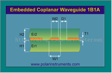
5. Embedded coplanar waveguide with ground 1B1A
Application: Single coplanar waveguide track in inner layers, the impedance track surrounded by VCC/GND zone, the next inner layer 2 is track layer. not reference layer of VCC/GND.
Presentation:
| H1 | The dielectric thickness between impedance trak layer and it’s following layer(inner layer 1:VCC/GND Zone) |
| H2 | The dielectric thickness between impedance trak layer and it’s following layer(inner layer 1:VCC/GND Zone) |
| W2 | The upper width of the impedance track(refer above configuration) |
| W1 | The bottom width of the impedance track(refer above configuration |
| D1 | The spacing of impedance track to it’s VCC/GND zone(in the same layer) |
| T1 | Thickness of impedance track=base copper thickness+plating copper thicknes |
| Er1 | The dielectric thickness H1 |
| Er2 | The dielectric thickness H2 |
6. Offset coplanar waveguide 1B1A
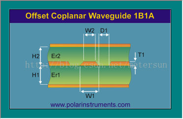
Application: Single coplanar waveguide track in inner layers, reference shield layer is VCC/GND zone in the same layer,and it’s next following VCC/GND layer.
Presentation:
| H1 | The dielectric thickness between impedance trak layer and it’s next following VCC/GND layer |
| H2 | The dielectric thickness between impedance trak layer and it’s next following VCC/GND layer |
| W2 | The upper width of the impedance track(refer above configuration) |
| W1 | The bottom width of the impedance track(refer above configuration |
| D1 | The spacing of impedance track to it’s VCC/GND zone(in the same layer) |
| T1 | Thickness of impedance track=base copper thickness+plating copper thicknes |
| Er1 | The dielectric thickness H1 |
| Er2 | The dielectric thickness H2 |
If you need help with any of this, or you need Coplanar Waveguide PCB Fabrication and Coplanar Waveguide PCB assembly, please give us a call or send an email to [email protected] to present your design problem. We’ll be happy to help you to get it right the first time.