What Is Wave Soldering?
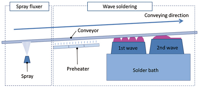
Wave soldering is a classic THT soldering process used for mass PCB assembly production containing through-hole-technology components. In this in-line process, a printed circuit board is passed through a wave solder machine with the solder material pre-loaded in, and the machine controls the height of the standing molten solder wave as well as the amount of time each circuit board spends in contact with it to stabilize soldering quality. As the circuit board with components inserted in is passed cross the machine, the liquid solder can generate contact between the component pin and the surrounding pad, then quickly forming a conductive solder joint. The complete process of wave soldering assembly involves some additional steps except submitting printed wiring board (PWB) to the wave:
1. Flux application: The flux is applied to the entire surface of the circuit board by means of a spray jet to ensure the cleanliness of the soldering site. As flux has the excellent feature of removing oxides and impurities from metal soldering PAD, preventing the formation of new oxide layers, and increasing the wettability of the solder to the soldering surface, which assists with joint generation and structure. But, Excessive flux will take the reliability risk of voids, although good wettabiltiy obtained.
2. Preheating: The aim of this process it to preheat the printed circuit board it pass over the solder module. The purpose here is to bring up the PCB to high temperature to get enough thermal to avoid thermal shock when it comes into contact with the high temperatures of liquid molten solder.
3. Wave solder: It is the process that the printed circuit boards pass through a wave of molten solder with careful temperature controls. In this way, the eutectic point of the soldering material will be activated and the circuit board can be soldered in a matter of seconds producing soldering joints that are reliable mechanically and electrically.
4. Cooling: This process is conversing to the preheating phase, the circuit board will slowly and smoothly go down to be cooled to room temperature. The slower quenching rate is to avoid warpage to the assembled circuit board and release enough time for the solder joint to solidify due to that the forced cooling directly after the dwell may cause unequal shrinkages. However, the assembled boards hate to be exposed to elevated temperatures any longer than necessary to eliminate potential damage to the board and heat-sensitive components.

Wave soldering is an efficient and economical process for the mass production of electronic assemblies using through-hole technology (THT) for many years. It is not suitable to the circuit board designed with very fine pitches any more.
But, it is still ideal for the many boards still designed and manufactured with conventional leaded components and some surface mount circuit boards that use larger components, such as power supply circuit board. Meantime, lead-tin solder was the public standard in soldering field for years, but RoHS compliance has regularly eliminated this in consumer electronics.
While a health issue, leaded solders can provide the excellent ability performance to prevent the formation of whiskers (extrusions of metal from the surface thought to arise to relieve intermetallic strain), which can take risk of shorting of electronics and a reduction in the assembled electronic board’s lifetime reliability. Solution to this, solder material with alloy compositions such as SAC (tin, silver, copper) have been applied to RoHS-compliant assemblies as it’s excellent lead-free solder that is not as susceptible to whiskering as some other alloys,and friendly to environment.
However, tin-leaded assembly process still applied for the circuit bards boards which are used in lower volume and possibly more specialised products such as military, automotive,etc.
As a professional PCB assembly company confidence at high quality of electronics assembly, Weller Technology can provide assembly services both RoHS application and Tin-leaded.
