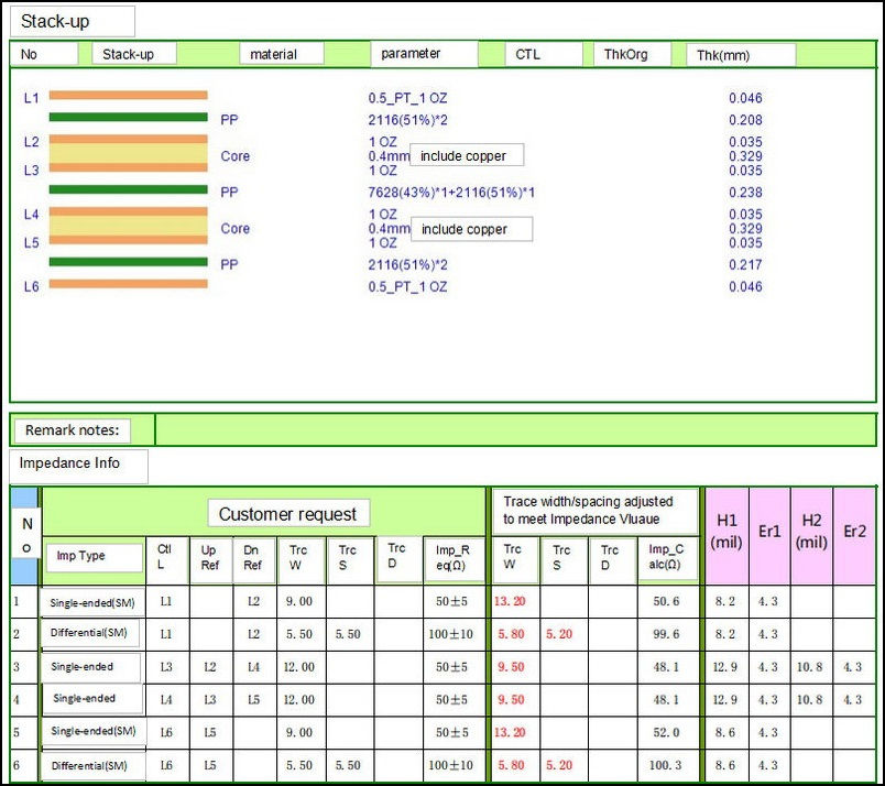
PCB trace impedance is the sum of all the resistance and reactance components of an electrical signal path. An ideal transmission line must have a characteristic impedance that matches both the transmitter and receiver of the intended signal. If the characteristic impedance of the matched transmission line is faithfully maintained, then the full signal sent by the transmitter is seen by the receiver at the end of the trace. There would be no reflection or attenuation of the signal. The full amount if signal power is absorbed by the receiver. For mismatched impedance, a reflection will occur at the far end and the complete signal will not be seen accurately at the receiver destination. Therefore, in practice, the details of the impedance control within the system need to be carefully considered.
For single-ended line transmission of an I/O signal, a 50 ohm impedance is often the required matching characteristic. The characteristic impedance of the signal path is a continuous 50 ohm path relative to the closest ground. The signal will return on the nearest ground path to the trace. Several applications have specific impedance requirements other than 50 ohms, based on legacy standards. Analog CATV video signals require a 75 ohm single-ended characteristic impedance, for example.
At higher frequencies, the PCB signal trace impedance will depend on the geometry of the circuit, so it has to be calculated. These calculations are complex. The impedance will depend on 4 parameters:
- Height (H) of the dielectric stack of material used between the signal trace of interest and the signal return plane. Keep in mind that the signal return could be on the same plane as the signal, as in a coplanar waveguide, or may be on a different plane.
- The trace conductor thickness (T)
- Width (W) of the signal trace conductor material. Outer PCB traces are often plated, providing a 20% uncertainty in exterior traces.
- Dielectric constant (Er) or relative permittivity of the material chosen for the PCB design. The dielectric constant is a measure of the electrical characteristics of the dielectric material. It is fixed once the material is chosen for your PCB. A typical value for FR4 may be 4.4. Small variances in Er can have a large impact on the final impedance tolerance. Only certain specialty materials have well-defined dielectrics.
The impedance of traces is defined by more than only the size of the trace. When a trace is defined to require controlled impedance, the accuracy of the impedance itself is of higher importance than the geometry of the layout feature. In order to maintain the impedance accuracy, Macrofab may change a trace width, trace height, or dielectric thickness given in the layout Gerber file. This will ensure that the final impedance is within the tolerance.
PCB Prepregs Materials
Prepregs are semi-cured materials used as bonding materials between two core laminates within a PCB. After the lamination step in the manufacturing process, the final thickness of the prepreg depends on the percentage of copper in adjoining conducting layers, the height of the copper, and the specific type of the prepreg used within the design.
Impedance-control
During the lamination process, a high degree of process control and integrity must be maintained. Post-lamination thicknesses of prepregs are reasonably predictable. The resin content of the PCB material is important as the percentage of the resin content has a great impact on the final thickness. The higher the thickness of the dielectric material, the lower the dielectric constant of the PCB material will be.
High-speed materials have lower dielectric constants and are suitable for applications requiring transmission of high-speed signals, usually having signal frequencies above 500 MHz. A layout designer must include the impedance information in the fabrication drawing notes and tables. The information should include the impedance value, the trace width, the spacing for differential pairs and the layer on which the control impedance traces are routed.
How to calculate the impedance?
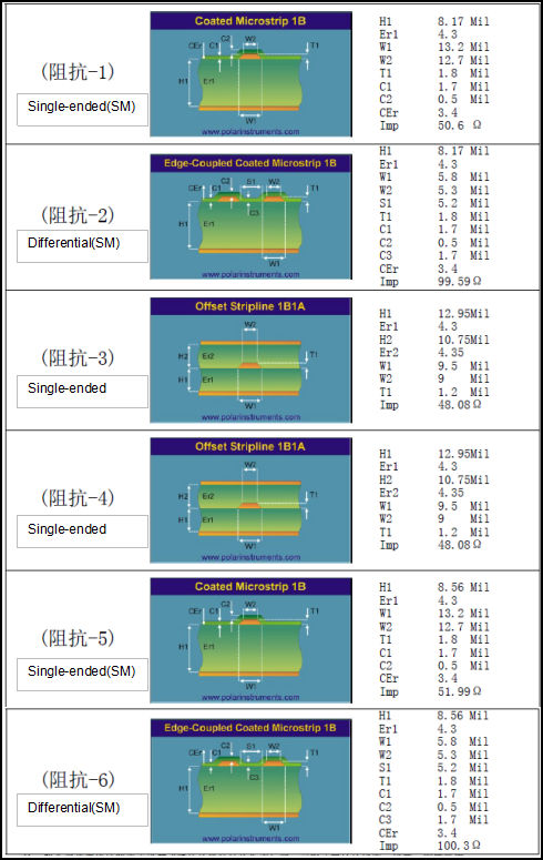
The calculation impedance software Polar Si9000 is popular in the PCB manufacture in present. Let me introduce it simply as below:
The width of the trace and height of the dielectric stack-up can be adjusted as needed in order to maintain the tolerance across a signal transmission line for +/- 10% of the ideal impedance value. Achieving this accuracy requires a good understanding of the Er values and experience about how dielectric laminates behave.


H1=> 8.17mil is the PP thickness between impedance trace layer and reference layer,it is 0.208mm per stackup at here.
Er1=>4.3 is the base material PP’s dielectric constant
W1=>13.2mil is the calculation trace width(the adjusted trace width,need to adjust trace width to meet impedance)
W2=>12.7mil is the upper trace width, after etching the trace will be like a Trapezoid,this determined by the copper thickness(trace thickness)
T1=>1.8mil is final nominal copper thickness
C1=>1.7mil is nominal S/M thickness
C2=>0.5mil is nominal S/M thickness on trace corner
CEr=>is S/M’ dielectric constant
Imp 50.6Ω=> is the impedance calculated theoretical
When the material is specified by PCB designer, the Er value is fixed. usually the normal FR4 Er value is about 4.1–4.7. The Er bigger the impedance value will smaller.
If there is no stackup required in the PCB manufacturing specification file, we can desgin a stackup (adjust the H1, inner layers is H1,H2) to meet impedance value. but sometimes there are many groups impedance in same layers, due to Er and H1(H2) have fixed, we need to adjust trace width(spacing) to meet all of the impedance value, otherwise, some groups impedance value can’t be meet.
If customer provide the stackup, The H1(H2) have been fixed, if the impedance calculation can’t meet the required value, then we will suggest to change the trace width(spacing) or to change H1(H2) PP thickness to ensure impedance vlue.
Sometimes the impedance trace width have been specified in specification of PCB FAB drawing, but can’t search the trace from gerber, or some impedance trace in gerber have no reference layer(or lots of the parts have no reference), such trace can’t meet impedance.
For the differential pair impedance trace, If the parallel lines spacing not fix, the actually value of them will exist distortion(some part the impedance value will out of tolerance).
Usually all of the impedance trace sample will be an impedance test coupon added. In coupon the differential pair trace spacing is completely same, when the value on test coupon are ok,there will be considered the impedance have been controlled OK.
If you have any question on trace impdeance before you design a comlex PCB board, you can contact us by [email protected]