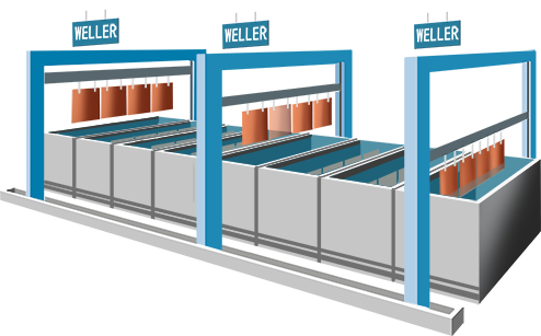
When you order PCBAs from WELLER, you are buying quality that pays for itself over time.

Our team will double review the terms and specification presented or related in your order. This is to make sure your product specifications and quality controls are thoroughly understood by us, and to ensure that the product delivers what it promises.
WELLER will not change any specification unless get official approval from customer. This action are far more stringent than those of other suppliers.
IMQC (incoming material check), this is to have a global inspection to incoming material (component, PCB board,stentcil tooling),to make sure each material match the specification.
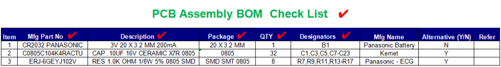
WELLER’s value: we always perform the BOM check list to make sure that the incoming components 100% conform it’s specification in BOM, and the size match it’s pattern on the PCB board.
All the components must be original parts as customer specified, no any alternatives without customer’s official approval.
This is a premise but core work to make sure the production moved forward correctly.
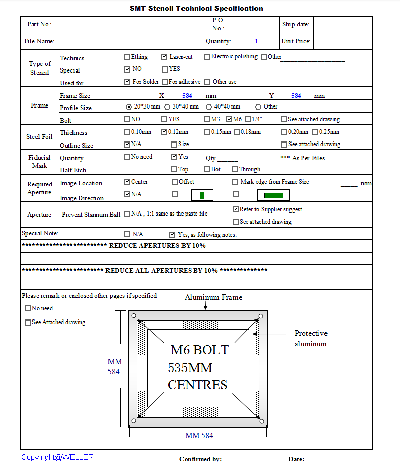
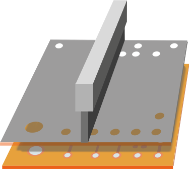
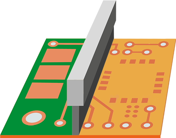
It is a tooled aluminum foil (or stainless steel foil) with opening window cut by laser, to simply transfer the solder paste via this window to the surface of SMD pad on the bare circuit board.
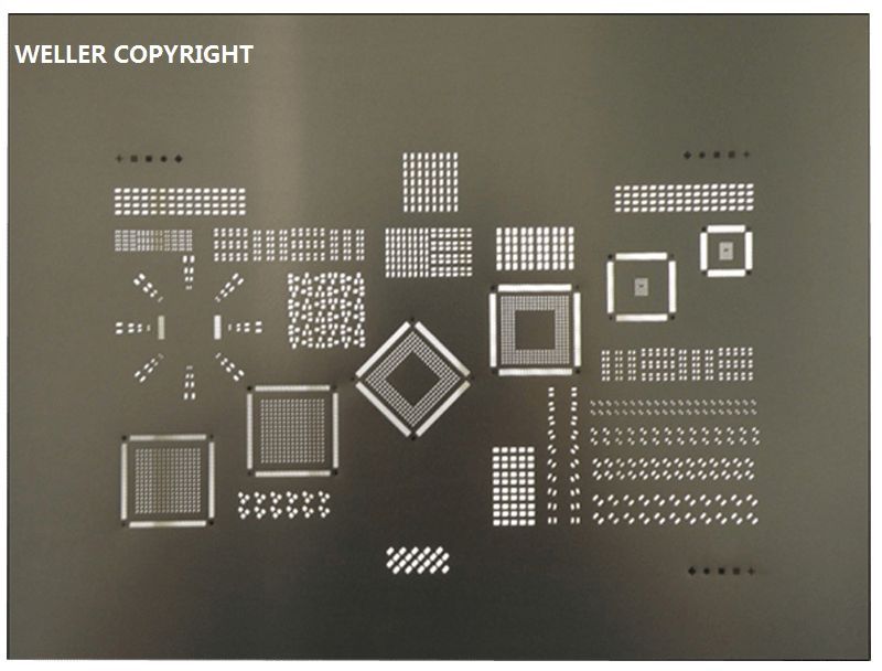
The quality of stencil is most important of high quality PCB assembly, all WELLER’s stencil is tooled by high quality of aluminum material with high precious laser cut process with REDUCE ALL APERTURES BY 10%.
Refer WELLER-SMT-Stencil-Technical-Specification
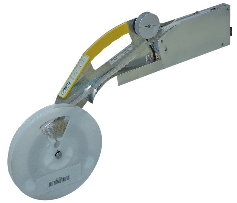
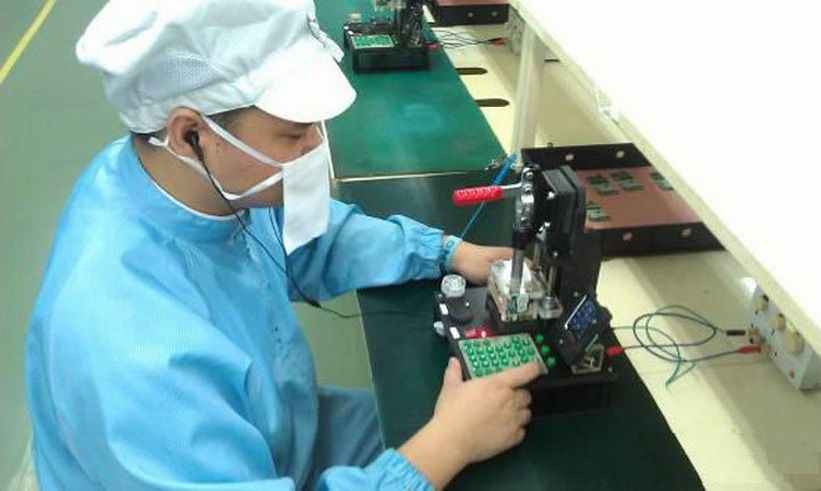
It is to load all the purchased SMD components by roll or tape into the feeders of SMT machine, the feeder location must conform to the components in pick and place file.
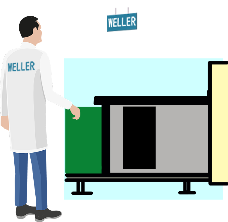
It is to transfer bare PCB board to the assembly process automatically.
All the bare PCB board load machine in WELLER is automatically controlled rather than manual transferring work in other supplier.And,this directly lead to the production efficiency and capacity improved.
Solder paste printing is a core step in the SMT (Surface Mount Technology) assembly process.
It is to print the solder paste via stencil on the every one of the pads on the PCB board which need to be components soldered on. This work normally done by high quality solder printing machine or by manual work.
The two key points on this process is paste print machine and the material of solder paste.
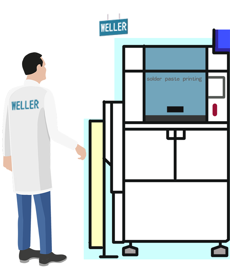
In WELLER, All the soldering printing work is done by automatic machine which have high-accuracy positioning and high-speed printing and highly stable quality than other suppliers who do this by manual work to avoid affording the high cost of buying Auto-printing machines.
And, all the solder paste we used is from ALPHA-OM-340, which have a most stable quality than other brand solder paste. And can apply to different end application of products (industrial PCB assembly, communication PCB assembly, medical PCB assembly,etc)
SPI means Solder Paste Inspection in PCB assembly industry. It’s work purpose is to check the solder paste deposits on the SMD component pads of bare printed circuit boards (PCBs) before loading the components on it . This is to sort out the potential flaws from solder paste printing process before forma SMT assembly.
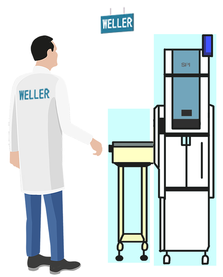
All the assembly lines in WELLER is matched with SPI machine, this is much more safe and high quality rather than most other suppliers who do not use any SPI or just make solder paste inspection by eyes.
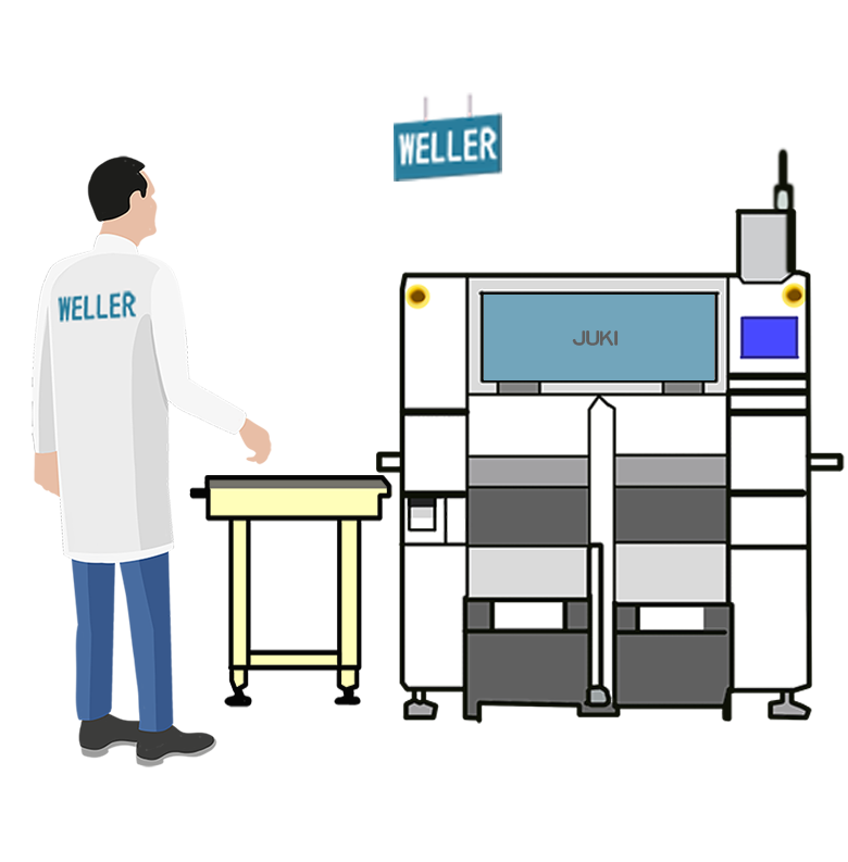
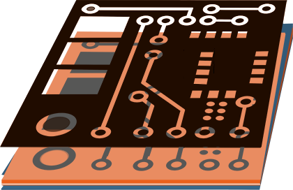
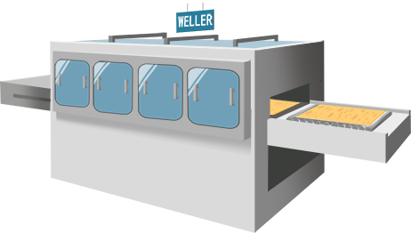
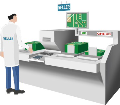
SMT (surface mounted technology) assembly is one of important part of PCB assembly process.
It is to mount the electrical components (surface mounted device) onto the surface of a bare printed circuit board.
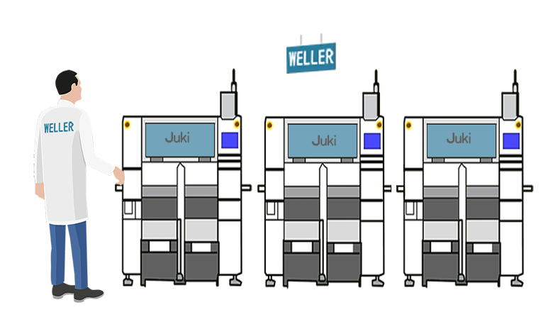
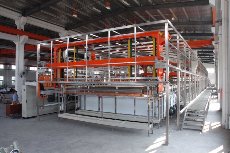
In WELLER, all the SMT machines in production line is from Juki with it’s latest model to ensure high accurate and high efficiency production work.No eed to subcontract work to outsource which other supplier do.
Universal SMT assembly which is a supplement to the regular assembly.
This is to assemble some un-regular shape size of components by unique assemble machine.
The production efficiency can be highly improved by this universal assembly optimizing process.
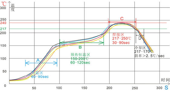
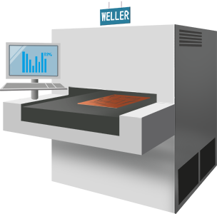
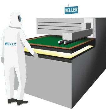
Reflow soldering is an important part of assembly process by which the molten state solder paste will turn to the permanent solder joints. So as that the SMD components is soldered on the SMT pad of the bare printed circuit board.
After this process, the components has been fully soldering jointed with it’s SMT pad under them.
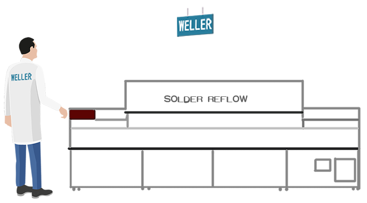
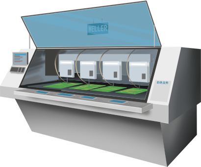
In Weller, we are using latest 12 temperature zones solder reflow machine to ensure the high quality soldering performance, especially for some fine pith and high density BGAs. And, all production record of soldering profile is kept 1 month at least for available traceability unless spherical request from customer. Which is better than other suppliers who do not have any production record backup.
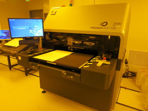
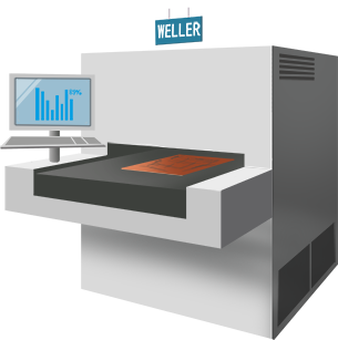
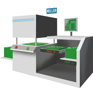
AOI (Automated optical inspection) is an important step of inspection in circuit board assembly process, it is an automated visual inspection of PCB(printed circuit board) assembly where a camera autonomously scans the SMD components under test for both catastrophic failure (e.g. missing component) and quality defects (e.g. fillet size or shape or component skew). This is a critical inspections process to ensure good quality of PCB assemblies.
In Weller, all the assembly production lines is equipped by AOI machine. All the PCB assembly production (even each prototypes) is implemented AOI inspection, rather than other suppliers who use manual power (by eyes) to have a visual inspection to the board.
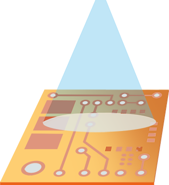
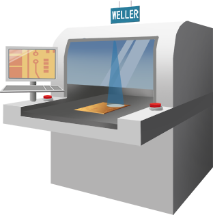
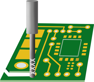
Automated X-ray inspection (also called AXI) is another important part of PCB assembly process;it is a technology based on the similar principles as automated optical inspection (AOI).
It is to uses X-rays as its source to automatically inspect the defects or features which are typically hidden from the positive view.
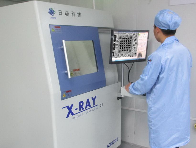
In WELLER,all the assembly soldering on BGA component, fine pitch components and QFN components must be done with X ray inspection with the machine equipped at our own house, and all the inspection record is backup in our system available for traceability. Rather than other supplier who do not have x-ray inspection machine and have to subcontracted it to outsource or do not do X-ray inspection at all and pass the defects or failures the customers.
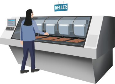
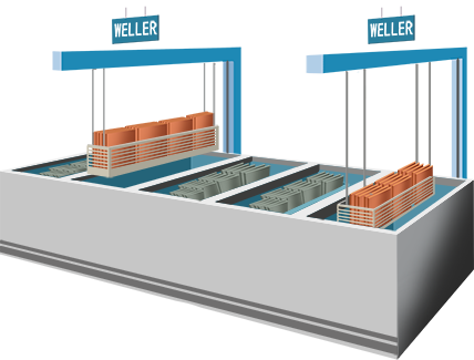
PCB Dip assembly is also called through hole components soldering process, it is to assemble though hole components by peak wave soldering process or by manual soldering work.
In WELLER, we have our own peak soldering process at house, this will improve the production efficiency and capacity accordingly once large amount of DIP production requested from customer.
So this will be the time saved and quality controlled rather than the other supplier who subcontracted this process to outsources.
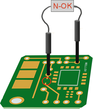
Functional test is to power on the assembled PCB board with firmware programmed in.
This is to dig out some hidden problem which escaped from the inspection in AOI and X-ray. This is best safe option to make sure customer to receive the ordered PCB assemblies at correct quality.
In WELLER, commonly we suggest customer to accept our request to firmware and power on their boards to implement a electrical function test, and do repair once some defects found at our house accordingly. So as that all the problem can be killed at our own house and not let them go to customer. Rather than other supplier who do not do any recommendation of functional test and the projects sometimes catch file when customer power on their boards after receipt.
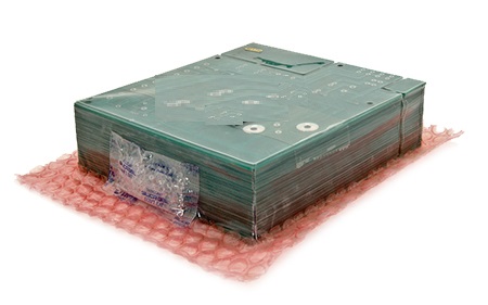
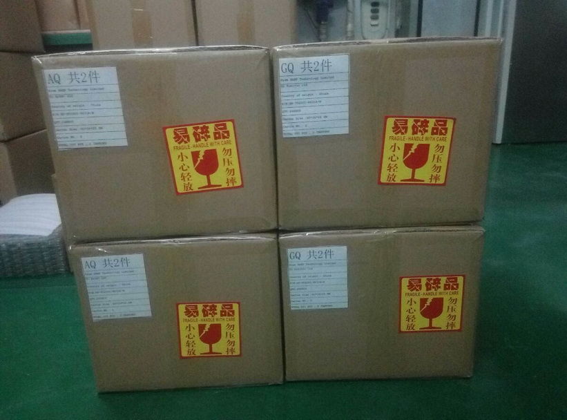
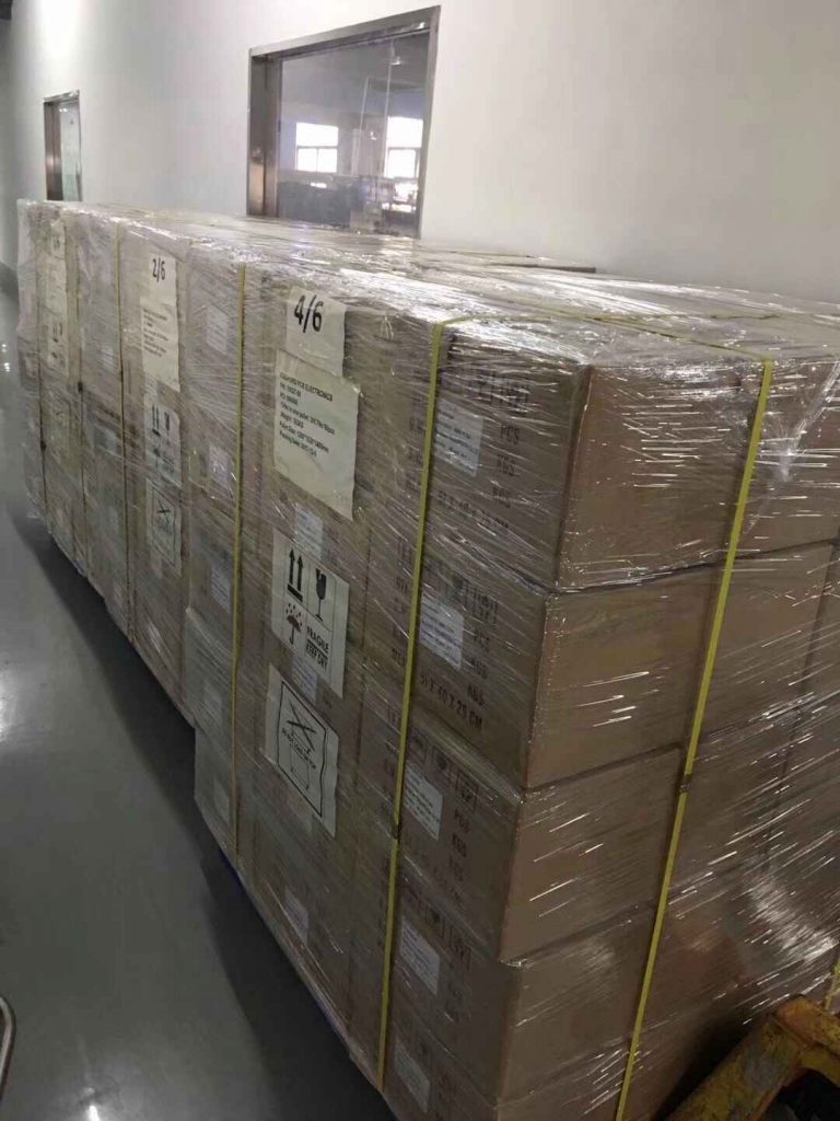
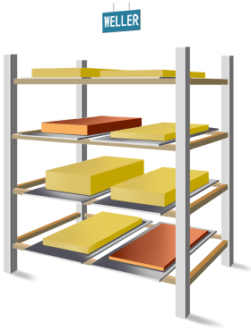
All the PCB assemblies from Weller is packed in ESD bags based material friendly to environment.
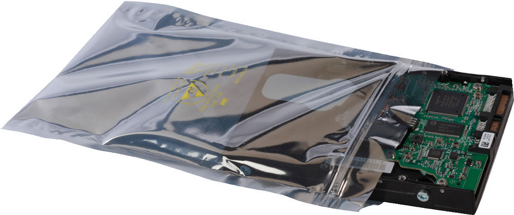
And, all the carton box package must be enough strong defend the stock and potential damage from delivery process.
Customer provide PCB files (Gerber file is a best option of document for manufacturer’s optimizing) with PCB specifications. The engineer in the Weller Team will perform verify the design and the specification against our manufacturing capabilities. Any change or modification issued in Weller must be approved by customer before manufacturing.
Weller’s value: Experienced engineer + the leading PCB pre-production CAM system Genesis 2000 to handle your data to ensure the work in security from the very start of the process. Will not change customer’s design or specification unless get customer’s approval.

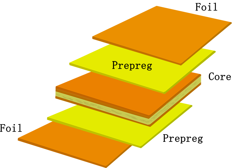
Base material is one of the key points that related to final PCB quality especially talking multilayer PCB. The quality of base material is mostly subject to it’s price.
Here are there are many unknown or local brand material with low prices but unstable quality(such as delamination for multilayer PCB assembly and voltage leakage for final functional PCB),some of them even not certificated by UL.
Weller: No matter that it is prototype PCB or mass production,unless customer’s prices pressure to use poor quality base material, or else We only use internationally known base material such as Shengyi, ITEQ,Nanya,Kingboard,Rogers, etc. All base materials WELLER used is certificated by UL, rather than other suppliers who use some inferior grade of material which is out of standard of UL.
It is also called the inner imagine transferring in a clean room, it is to transfer the PCB circuit image by using an artwork film to the circuit board surface, using photosensitive dry-film and UV light, which will polymerise the dry film exposed by the artwork.
Weller:
The grade of clean room: 100 000;
The high quality of artwork film imported from Japan.
This is to remove the unwanted copper from the working panel by using chemical etching.
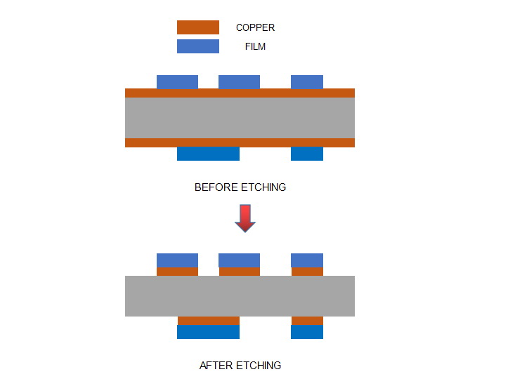
After the unwanted copper has been removed, the remaining dry film is then to be removed off and leaving behind the copper circuitry that matches the circuit design.
WELLER’s Value:
Advanced automatic control etching production line with high deficiency work from start to end without any manual process.
Through scanning of the production circuit board to catch out the defects via comparing the exist circuit against the digital “images” from original design.

The purpose of this stage is to sort out the defects PCB in inner layers production, and do not leave it to next production process.

WELLE’s value:
Latest leading AOI machine+90% automatic running instead of manual scanning work.
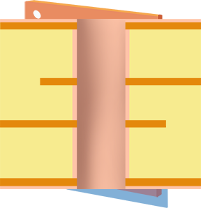
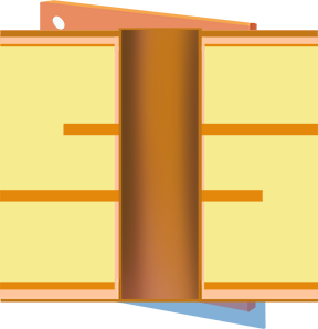
It is to “stack ”inner layers,prepreg (which is for insulation purpose) and copper foil of out layers (top and bottom) together.
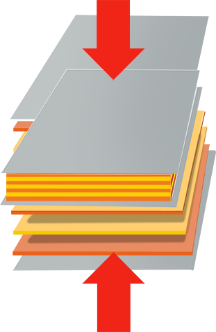
It come out by using a combination of specific temperature(heat and cooling), pressure for a specific time to allow the resin within the pre-preg to flow and bond the layers together to form a solid multilayer panel.
Normally,there are many times of lamination process for some multi-stacked via and blind holes.
PCB layers stack up is critical to multilayer PCB,WELLER will not change customer’s stack up unless get official approval from customer. This action are far more stringent than those of other suppliers.
It is to subsequently drill the holes within the multilayer PCB via the drilling machines.
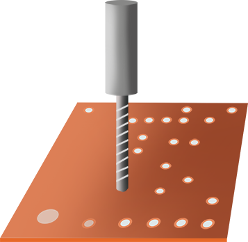
This process must be highly optimised so that it can meet the registration positional accuracy to all of the the inner layer connections.
Eexcept the mechanical drilling process,the drilling can also be done by a laser drill for blind holes (LASER CO²+LASER UV).
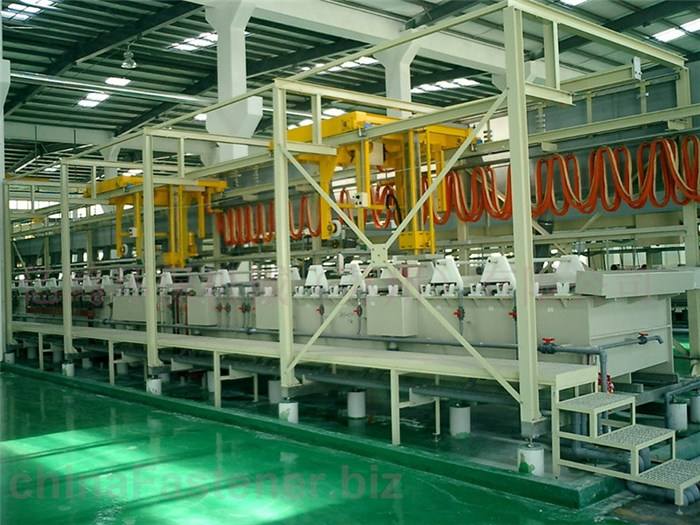
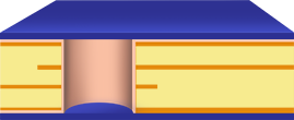
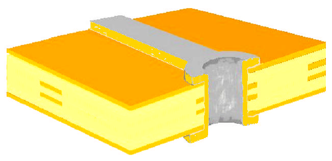
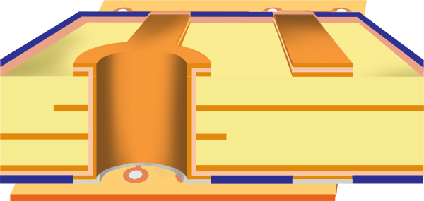
PTH also called Plated Through Hole: the purpose of this process is to plate thin copper (normal thickness is 0.3-0.5um) to the wall of the through holes by A complex chemical process to get the basic electrical connection to the layers.


Panel plating after PTH process is to plate 5-8 um extra copper to the surface of PTH copper. This is to protect PTH copper from damage during the next following up process.
WELLER:
Copper thickness on through plated hole: 25um(min). Which is the same standard of IPC class 3.
Or else, the poor thickness copper on the through plated hole will take risk of open circuit after high temperature of assembly process.
The similar process as the inner layer’s (perform the image transfer by using photosensitive dry film, exposure to UV light and etching).Only with one main difference:the dry film where we want to keep the copper/circuit track will be removed– so as that we can plate additional copper later in the process.
This step of the process is performed in a high grade clean room.
The detail of steps of outlayer imagine process is as below:
Dry-film Resist Coating Outer Layer Panels
The same resist or light sensitive film used on the inner layers is used for the outer layers. The film covers the entire surface including the drilled holes.
Outer Layer Expose & Develop
After dry film lamination the panel is exposed and developed using the same procedure used for the inner layer cores. Clear areas in the film allow light to pass through and harden the resist creating an image of the circuit pattern All of the drilled holes that are exposed will be plated through.
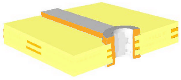
Copper “Pattern”Plate
The electroplating processes that electrically plates copper onto the exposed metal surfaces is next. The copper will be plated up to a thickness of approximately 1 mil (0.001”), depending on the required final finish for the panel.
The copper plating step is followed by plating tin onto all the exposed copper surfaces.

The tin will be used as an etch resist to maintain the copper traces, hole pads and walls during the outer layer etch process.
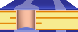
This is second electrolytic plating stage that to electrically plates copper onto the exposed metal surfaces ( in areas without dry film (circuitry)).
By this process,the copper will be plated up to a thickness with and average of 25um / min 20um through the hole. Once the copper has been plated, tin is applied to protect the plated copper(which will be il).
WELLER’s standard copper thickness of through hole is 25um (nominal), which equates to IPC class 3,this thickness can provide much more greater reliability of the via structure and improved z-axis expansion performance.
3 basic steps in pattern plate process:


This is simply a three step process.
The first step is to remove the blue dry film to expose the unwanted copper.
The second step is to etch away the exposed/unwanted copper but now the tin deposit acts an etch resist protecting the wanted copper.
The third and final step is to chemically remove the tin deposit leaving the pads and traces on the panel surface.
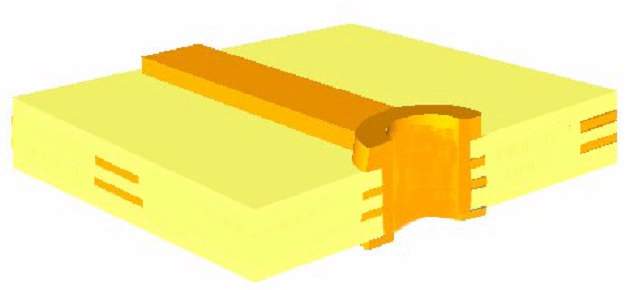
Then the tin is chemically removed leaving behind a bare copper and laminate panel. The surface pads, traces and plated through holes are the exposed copper. This is the last step in strip-etch-strip.
Similar with inner layer AOI the imaged and etched panel is scanned and compared to make sure that the circuitry meets design and that it is free from any defects.
WELLER do not allow to repair any welding or open circuit.
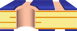
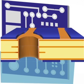
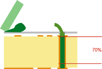
It is to plug the via holes by solder mask or by resin performed in a clean room.(Or fill the via holes with copper,which is another process).

How to do this? By screen printing to push soldermask into holes – a separate operation using an aluminium stencil.
WELLER perform the plugging criteria with 70% filling per hole. This is to eliminate the risk of “broken” circuit path after high temperature in assembly process.
Soldermask ink is coated over the whole PCB surface. By using artworks and UV light we expose certain areas to the UV and those areas not exposed are removed during the chemical development process – typically the areas which are to be used as solderable surfaces. The remaining soldermask is then fully cured making it a resilient finish.
This step of the process is performed in a clean room.
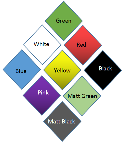
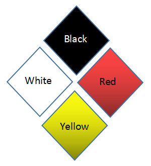
Common PCB silkscreen color: Green, black, white, blue,yellow,pink,red,matte green, matte black.
The primary purpose of the mask is to restrict the areas that will be covered with solder. It also protects panels from contamination, handling damage and possible electrical shorting during assembly and installation.
Importance: With ≥ 5um on the knee of the track and between 10-30um on the surface. The thickness of solder mask is critical to improved electrical insulation and resilience to chemistry or mechanical force that could cause loss of soldermask.
At WELLER,we always keep using high quality of soldermask material such as Taiyo-PSR-4000 to print the PCB board.
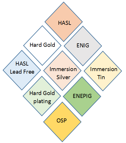
Various of PCB surface finishes are used to coat the exposed copper areas. This is to enable protection of the surface and good solderability.
The various of finishes can include Electroless Nickel Immersion Gold, HASL, Immersion Silver,ENEPIG etc.
Thicknesses and solderability tests are always carried out.
Commonly available PCB surface finishes in Weller (all in house)
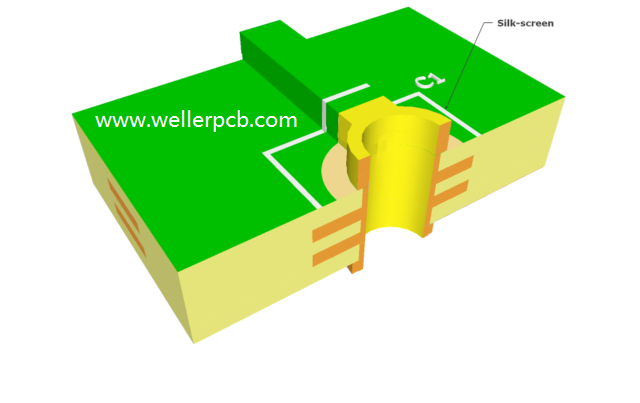
Non-conductive epoxy ink is silkscreened onto one or both sides of the panel depending on the requirements of the customer.Or, it is printed out by laser machine.
The printing usually dictates the component placement, part number or name, date code, logo or other specified information. PCB Panels are then baked to cure the ink.
Common PCB silkscreen color: White,black,red,yellow.
WELLER normally use silkcreen ink Tamura DSR 330 to ensure a high quality of legend printing. And we are upgrade the printing machine to laser printing to get a bettter quality.
After surface finishing process,then the boards are cut to size on a CNC machine or router.
Most panels have the individual parts routed out into single pieces or arrays of varying sizes. Boards or arrays can also be scored so that they can be easily broken apart after assembly.
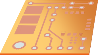
PCB boards are tested for opens and shorts in the circuitry, in one of the last steps of production.
Test programs can be loaded directly onto various types of test machines or used to create specific fixtures and test programs.
PCB boards are visually inspected to assure they meet our customers’requirements, industry specifications (IPC class 2 or class 3) and WELLER’standards, as well as having the physical dimensions and hole sizes verified with a paper report with shippment to customer.
PCB Boards are vacuum wrapped using specific materials that made from renewable resource materials. To assure the boxes can not be damaged during transport.