The meaning of PCB impedance ?
The meaning of PCB impedance ?
PCB impedance is the combination of the capacitance and inductance of a circuit when operated at high frequency. Though also measured in Ohms, it is somewhat different than resistance which is a DC characteristic. Impedance is an AC characteristic, meaning that it is related to frequency, resistance is not.
The significance of impedance to PCB:
PCB can realize high speed data transmission, impedance matching is a necessary thing.
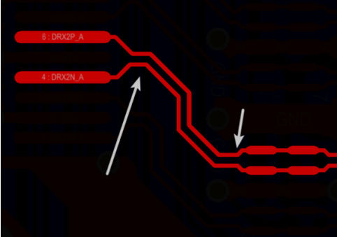
Taking the USB interface of mobile phone as an example, it can transmit data synchronously in two directions with high speed and low cost. The two most common types are type-A, Type-B and type-c. In the definition of USB protocol (D +, D -), (TX +, TX -), (Rx +, RX -) differential signal lines transmit digital signals. In order to ensure the stability of the transmission signal, PCB design differential line must be in accordance with the routing rules of differential signal strictly.
Some notes of multi layer PCB impedance line routing
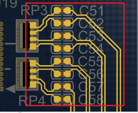
- The components PAD shall be arranged as close as possible, the distance between PADS shall be shortened to make the difference line as short as possible, and make via holes as few as possible.
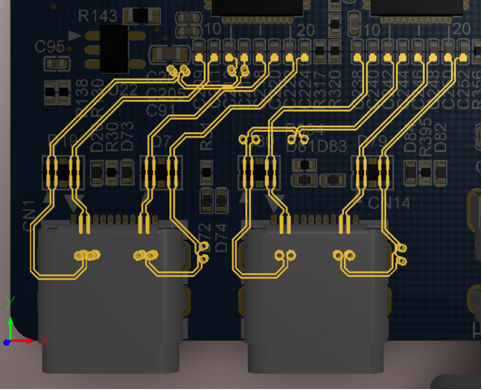
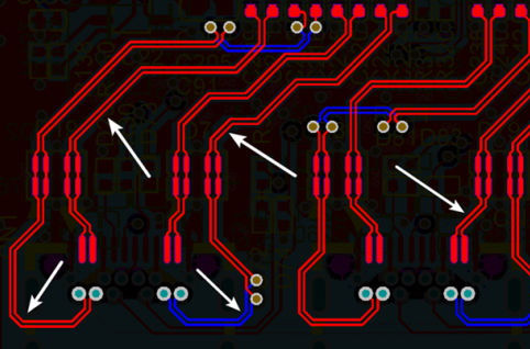
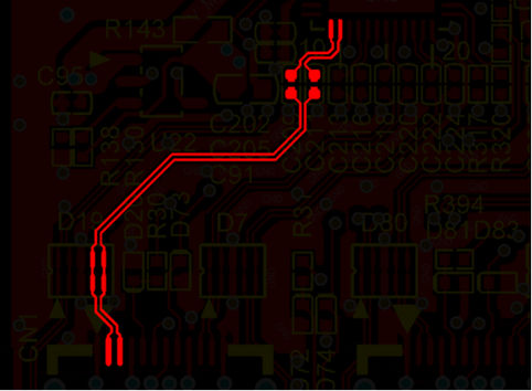
2. The route shall be parallel and symmetrical. It is not allowed to route the corner line at 90 ° but it should be with 45 ° or arc routing. The distance between the lines shall be controlled within 4mil.
3. When series resistance and capacitance, they should be aligned up and down or left and right.
4. Differential impedance lines should be equidistant and equidistant as much as possible to avoid timing deviation and common mode interference.
5. Because of the pin distribution, vias, and routing space and other factors, the differential impedance line length is easy to be mismatched. Once the line length is mismatched, the timing will shift, which will reduce the signal quality. Therefore, the corresponding compensation should be made for the mismatching of differential pair to make the line length match. The length difference is usually controlled within 5MIL, and the compensation principle is to compensate the parts where the length difference occurs.
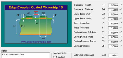
The impedance calculation software we use is polar si9000, and the parameters are as follows:
H1: dielectric thickness (thickness between impedance line and reference layer)
ER1: dielectric constant of plate 4.2-4.6 (PP is calculated as 4.2, core is calculated as 4.5)
W1: design line width
W2: upper line width = design line width minus 0.5mil
S1: distance between two lines
T1: copper thickness, calculated by 1oz (1.4mil) in general
C1: C1: thickness of green oil on the substrate surface
C2: thickness of green oil on copper foil surface
C3: thickness of green oil on the substrate surface
CER: dielectric constant of green oil 3.5
For more about PCB impedance,you can freely contact us by [email protected].