What is The PCB Impedance?
PCB impedance is the combination of the capacitance and inductance of a circuit when operated at high frequency. Though also measured in Ohms, it is somewhat different than resistance which is a DC characteristic. Impedance is an AC characteristic, meaning that it is related to frequency, resistance is not.
What is The PCB Controlled Impedance?
Unless you have carefully designed the trace and its environment, impedance is typically “uncontrolled”, meaning that impedance will vary in value from point to point along the trace.
At high frequencies, PCB traces do not behave like simple connections, controlled impedance helps us ensure that signals are not degraded as they route around a printed circuit board.
Essentially, controlled impedance is the matching of substrate material properties with trace dimensions and locations to ensure the impedance of a trace’s signal is within a certain percentage of a specific value. Controlled impedance boards provide repeatable high frequency performance.
When to Use Controlled Impedance
When a signal must have a particular impedance in order to function properly, controlled impedance should be used. In high frequency applications matching the impedance of PCB traces is important in maintaining data integrity and signal clarity. If the impedance of the PCB trace connecting two components does not match the components’ characteristic impedance, there may be increased switching times within the device or the circuit. There may also be random errors.horizontal
What Determines Controlled Impedance?
The characteristic impedance of a PCB trace is typically determined by its inductive and capacitive reactance, resistance, and conductance. These factors are a function of the physical dimensions of the trace, the dielectric constant of the PCB substrate material, and dielectric thickness. Typically PCB trace impedance can range from 25 to 125 ohms. The impedance value generated from the PCB structure will be determined by the following factors:
– Width and thickness of the copper signal trace (top and bottom)
– Thickness of the core or prepreg material on either side of the copper trace
– Dielectric constant of the core and prepreg material
– Distance from other copper features(signal shield layer)
Applications of Controlled Impedance
Controlled Impedance should be considered for PCBs used in fast digital applications such as:
– Telecommunications
– Computing 100MHz and above
– High Quality Analog Video
– Signal Processing
– RF Communicatio
What is Weller’s Experience with Controlled Impedance?
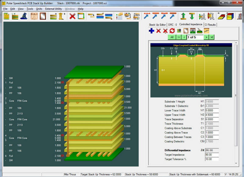
Weller uses impedance modeling software and impedance testing hardware to meet your controlled impedance requirements; Polar Instruments “SpeedStack” and “CITS” testing. This robust toolset incorporates both a high quality field solver and a comprehensive material library to ensure that you design is executed correctly the first time.

Example of Controlled Impedance
The most popular example of controlled impedance is the cable that connects the antenna to your TV. That cable may be a coaxial cable consisting of a round, inner conductor, separated from the outer cylindrical conductor commonly called the shield by an insulator. The dimensions of the conductors and insulator, and the electrical characteristics of the insulator are carefully controlled in order to determine the shape, strength and interaction of their electrical fields which will determine the electrical impedance of the cable.
How to specify PCB controlled impedance in your files to printed circuit board manufacturer?