Altium File
Altium Designer is a Printed Circuit Board and electronic design automation software package,which is widely used by electron designer and PCB manufacturer. It is developed by Australian software company Altium Limited,who developed another brand of PCB design software Protel. It is a powerful integrated electronic design software no matter what demand you need: HDI PCB design, embedded copper coin PCB design, PCB impedance, high frequency PCB design etc. But by now it only can be operated on windows system.
It is perfectly functional integrated with: schematic design,circuit diagram simulation, PCB edit,topology logical,auto PCB layout,Signal Integrity Analysis,and other technology such as design generation, etc.By using Altium designer,it enables electronic engineers to effortlessly and Qualitatively connect with every facet of the electronics design process.
Except inheriting the previous advantages and features of Protel 99SE, Protel DXP, the new Altium Designer has embedded some new improved function and high grade application.
It’s platform expand the traditional design interface for board to board. With global integrated design features from FPGA and SOPC,it enables electronic engineers to effortlessly integrate the designs of FPBA, PCB design, and embedded design development. Thus it require high powerful computer system due to the integrated extra design function on FPCB and embedded software with basically inheriting the previous advantages and features of Protel.
Simple 14 steps to build new project by Altium designer
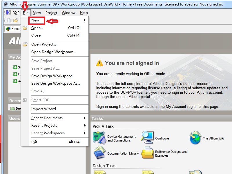
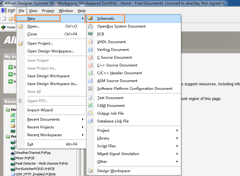
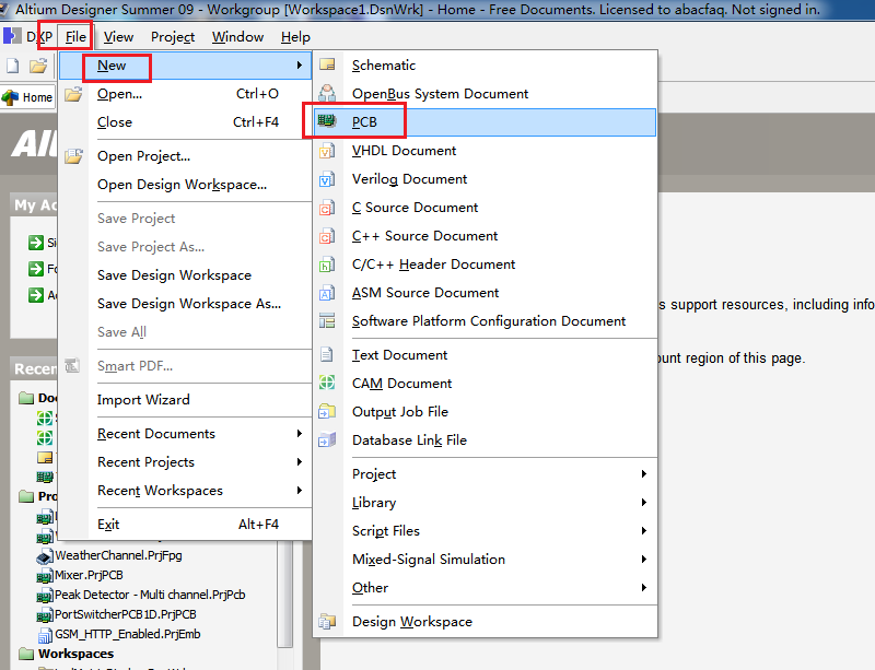
Step 1: Open the Altium designer on your desktop, and click main menu “File”–>”New”
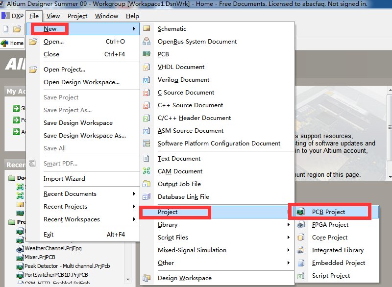
Step 2: Build new PCB project: File–>New–>Project–>PCB project.
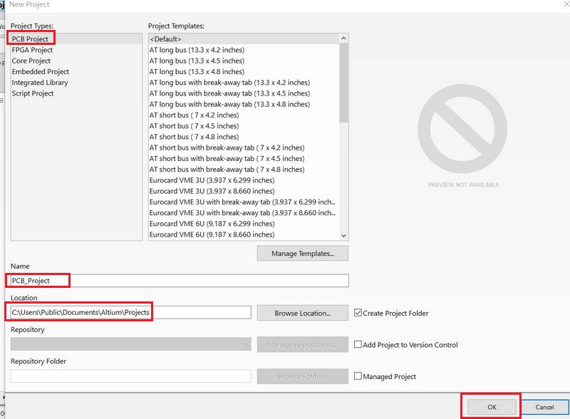
Step 3: Project information filling and Save
Step 4: Build new schematic diagram, main file menu–>file–>new–>schematic.
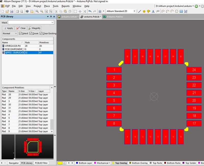
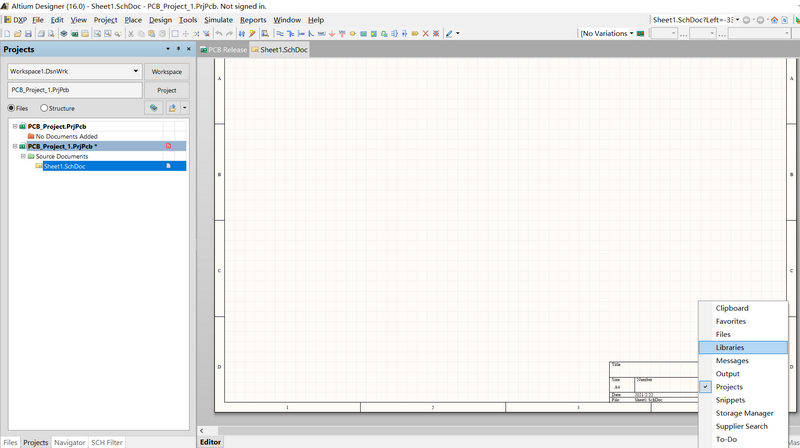
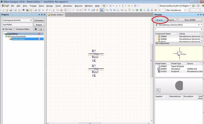
Step 5: place the components.
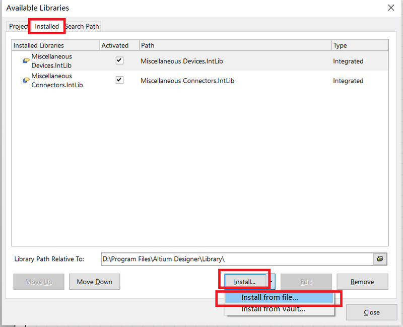
Step 6: Set the components libraries
Step 7: Add new components to libaries
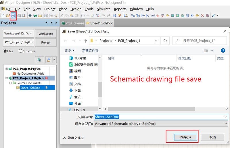
Step 8: Schematic drawing file save.
Step 9: Set up new PCB design project
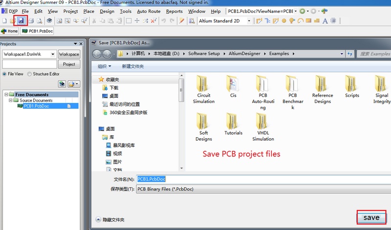
Step 10: Save PCB project files
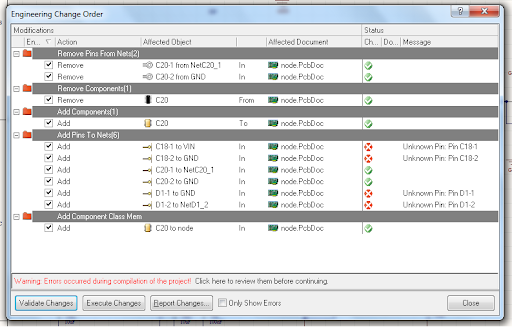
Step 11: Import schematic drawing to altium designer
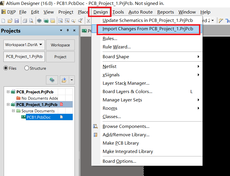
Step 12: Schematic drawing import
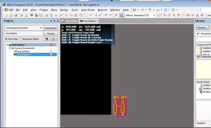
Step 13: Components placed sucessul
Step 14: Final step-enjoy your layout work