Founded in 2006, Weller Technology is Committed to provide leading manufacturing service of circuit board to our customers. Benefit from our continuous invest in advanced production equipment and skilled people, today we have the manufacturing capability to produce 2-50 layers PCBs, including standard PCB, prototype PCB, Rigid and Rigid-Flex PCB, Single sided and multilayer PCB, HDI PCB, backplane PCB, metal-backed PCB etc., and covered almost all types of substrate materials, including FR-1, FR-2, FR-4, FR4 Halogen Free, CEM-1, CEM-3, Hight TG, Aluminum, etc. with various types of substrates for a variety of applications including:
- Military/Aerospace
- Industrial
- Commercial
- Medical
- Telecommunications
- Consumer Electronics
- RF/Microwave
In this page, we will focus on traducing standard FR4 based standard PCB, about other advanced PCB techniques, you can also refer to our other technical articles .
Opposite to prototype PCB, standard PCB fabrication is streamline manufacturing and qualified with regular tolerance and technical requirements. That means they are PCBs can meet large volume manufacturing process.
When can you release it as Standard PCB Board?
PCB Design That Has Been double Verified and Optimized by Prototypes PCB:
It is worth to have your PCB design to have an exam by a prototype production process before you release it to large volume production. By verify the prototypes work, it can detect out potential flaws in your design so as that you have time to modify it and then move it to production. Sometimes the PCB designer needs multi-times prototypes to thoroughly eliminate all the flaws before formal production. Except detecting the design flaws, prototypes can also explore out some potential weakness of production. Actually, it is unnecessary to invest lots of money on PCB prototypes, but just time is saved and you can put it in your application directly, tolerance is under more strict control and products are well tested before shipping to you.
When You Must Use PCB Prototype?.
New Products Development:
If you’re developing a new electronic product, it is better to exam your ideas by physical prototypes instead of the drawing on the paper. Why not choosing Weller Technology? We can make your concept into reality with prototype PCB. At Weller Technology, we make prototypes PCB by restrict process as manufacturing standard PCB. So, manufacturing prototype PCB at Weller Technology will help you to avoid the flaws that are possibly appeared in mass production, and the lead time can be reached within 24 hours at the fastest.
Get to Know More About PCB Prototype
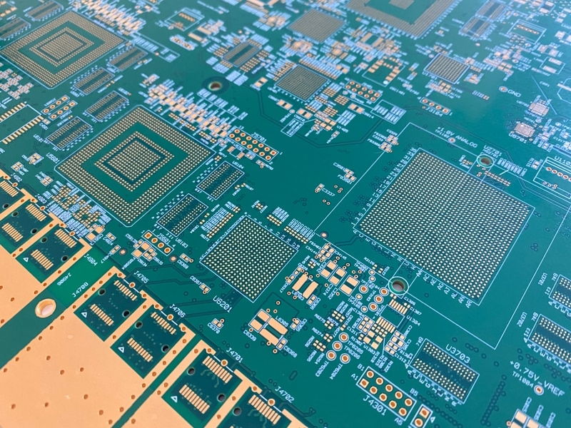
Standard PCB Capability
| Feature | Weller´s technical specification |
|---|---|
| Number of layers | 4 – 22 layers standard, 30 layers advanced, 40 layers prototype. |
| Technology highlights | Multiple layers of epoxy glass fiber bonded together with multiple layers of copper of varying thicknesses. |
| Materials | High performance FR4, halogen-free FR4, low loss and low Dk materials |
| Copper weights (finished) | 18μm – 210μm, advanced 280μm / 8oz |
| Minimum track and gap | 0.075mm / 0.075mm |
| PCB thickness | 0.40mm – 7.0mm |
| Maxmimum dimensions | 580mm x 1080mm, advanced 610mm x 1400mm |
| Surface finishes available | HASL (SnPb), LF HASL (SnNiCu), OSP, ENIG, Immersion Tin, Immersion Silver, Electrolytic gold, Gold fingers |
| Minimum mechanical drill | 0.15mm |
| Hole Tolerance | PTH: ±0.075, NTPH: ±0.05 |
| Solder Mask Color | Green/Black/White/Red/Blue/Yellow |
| Silkscreen Color | White, Blue, Black, Red, Yellow |
| Min Annular Ring | 3.0mil |
| Board Thickness Tolerance | ±0.1mm – ±10% |
| Board Size Tolerance | ±0.1mm – ±0.3mm |
| Copper Thickness Tolerance | +0μm +20μm |
| Inner Layer Copper Weight | 0.5oz – 3.0oz |
| Hole Plating Thickness | 20μm – 30μm |
| Plated Hole Size Tolerance | PTH: ±0.075 |
| Non-Plated Hole Size Tolerance | NTPH: ±0.05 |
| Aspect Ratio | 1:10 (Hole size: Board thickness) |
| PCB Eelctrical Testing | 10V – 250V, flying probe, Or testing fixture |
| Impedance Tolerance | ±5% – ±10% |
| SMD Pitch | 0.2mm (8mil) |
| BGA Pitch | 0.2mm (8mil) |
| Chamfer of Gold Fingers | 20, 30, 45, 60 |
| Solder Mask Bridge | 0.1mm |
| Minimum distance between plated holes and trace | >=12 mil |
| Minimum distance between plated holes and trace | >=12 mil |
| HDI builds | 1+N+1, 2+N+2, 3+N+3,4+N+4, any layer in R&D |
| Minimum laser drill | 0.10mm standard, 0.075mm advanced |
| Back-drill | Available |
| Depth-control drill | Available |
| Copper coin embedded | Available |
| Resistors embedded | Available |
| IPC Criteria | class 2, class 3 |
| MOQ | 1PCS |
Why produce Standard PCB from Weller Technology
Weller Technology always offer keeps standard lead times that are consistently faster than the industry, to support our customer’s requirements to beat their competition to market. we rest our customers assured with top quality, skilled expert, competitive price and good after-sale service.
Quality assurance:
- Qualification by ISO 9001: 2015, IPC, and UL standards.
- Bare PCB 100% visual inspection and mechanical AQL on IPC-600 class2 or class 3
- 100% electrical testing before shipping
Manufacturing facility and People
- 30+ experienced engineers for R&D team and 20+ overseas sales for business team
- 7 SMT Lines (13 million chips per day)
- 3 Production Lines (1.2 million pcs per day)
Price and cost
- Optimized solution will be always available per your requirements.
- Accountable material and components sourcing support with reasonable price
- Whole industry supply chain
Good After-sale Service
- One-to-one timely customer order status feedback
- Monitor and manage production by ERP system