Background
The quality of SMT soldering has a great impact on the life of any electronic product, and there are many reason of SMT soldering quality that are actually affected in the production process.The following are some main factors affecting SMT soldering quality.
1-BOM preparation
As one of the most important composite materials in SMT, the quality and performance of BOM is directly related to the quality of reflow soldering. The following points need to be considered:
A. The component package must meet the automatic installation requirements of the placement machine.
B. The component drawing must meet the requirements of automatic SMT because it must have a standard shape with high dimensional accuracy.
C. The solderable end of the component and the soldering end of the PCB pad should meet the requirements of reflow soldering, and the solderable end of the component and the pad will not be polluted or oxidized. If the solderable ends of components and PCB pads are subjected to oxidation, contamination or moisture, some soldering defects may occur, such as poor wetting, pseudo soldering, solder beads or cavities.
It can be measured using a humidity sensor. Humidity sensors must be stored in a dry box after vacuum packaging, and they must be baked before the next manufacturing.
2-Manufacturability design of PCB pads
According to HP statistics, 70% to 80% of manufacturing defects come from PCB design issues. For a PCB with the correct pad design, even if a slight skew occurs during the surface mounting process, it can be corrected by the surface tension of the molten solder, which is called the automatic positioning. However, if the PCB pad design is not correct, solder defects such as component position shifts and tombstone shapes can still occur even if the mounting position is very accurate. Therefore, the following aspects must be considered in the design of SMT pads.
A. The symmetry of the pad. In order to avoid the problem of position shift and tombstone after reflow soldering, for 0805 or lower chip components, the pads at both ends should maintain symmetrical pad sizes and heat absorption and heat dissipation capabilities to maintain a balanced solder with melting surface tension. If one end is on a large copper foil, it is recommended to use a single wire connection to connect the pads on the large copper foil.
B. Space between pads. In order to ensure a proper overlap size between the end of the component or the lead and the pad, when the space between the pads is too large or too small, solder defects are often caused. The remaining dimensions of the gasket must ensure the meniscus shape of the solder joint after the end of the component or the lap joint between the pin and the gasket.
C. The pad width should be basically compatible with the width of the component ends or pins.
D. Do not place through-hole vias on through-holes. Otherwise, during the reflow soldering process, the molten tin may flow along the through-hole vias, resulting in false soldering and insufficient tin. It may flow to the other side of the board and cause a short circuit.
3-Solder paste printing
The solder paste printing technology is mainly aimed at solving the incompatibility of the solder paste printing amount (filling amount and solder paste transfer amount). After the PCB is correctly designed, 60% of the PCB is used for rework due to poor solder paste printing.

4-Solder paste quality
There are two main aspects of solder paste quality insurance: storage and application. Solder paste is usually stored between 0 and 10 ° C, or according to the manufacturer’s requirements. For its application, the temperature of the SMT workshop must be 25 ° C ± 3 ° C, and the humidity must be 50% ± 10%. In addition, its recovery time must be 4 hours or more, and it must be sufficiently stirred before application so that its viscosity has excellent printability and release deformation. The solder paste cover must be properly placed after application, and the board on the solder paste must be reflow soldered within two hours.
For us-WellerPCB, we have been using solder paste as Alpha solder paste OM-340
5-Template design
Stencils are a must for printing technology, and their quality directly affects the quality of solder paste printing. So far, there have been three methods of making stencils: chemical etching, laser cutting, and electroplating.
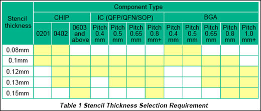
A. Stencil plate thickness. In order to ensure the amount of solder paste and welding quality, the surface of the template must be smooth and uniform, and the choice of the thickness of the steel plate should be determined by the component with the smallest lead pitch. The relationship between the thickness of the steel plate and the minimum spacing and composition values can be summarized in Table 1 below.
B. Aperture design. The hole is a trapezoidal section hole, and the opening is a bell mouth. Their walls are smooth and free of burrs. Aspect ratio = aperture width / stencil thickness (for Fine-Pitch QFP, IC); area ratio = aperture / basic area of hole wall area (0201, BGA, CSP parts).
C. Solder ball processing. The solder ball processing implemented on the template holes of 0603 or above CHIP components can effectively avoid the generation of solder balls after reflow. For parts with too large mats, grid separation is recommended to prevent excessive tin production.
D. Marking. The B side of the template should generate at least 3 MARK points, and the template should be compatible with the MARK on the PCB. There should be a pair of MARK points with the longest diagonal distance to improve printing accuracy.
E. Printing orientation. Printing direction is also a key control point. In the process of determining the printing direction, components with a good space between each other should not be too close to the track. Otherwise, the bridge connection may be caused by too much tin.
5-Scraper
Use a nickel-plated steel scraper, typically a 60 ° scraper. If there are through-hole parts, a 45 ° scraper is recommended to increase the amount of tin on the through-hole parts.
6-Print parameters
Printing parameters mainly include scraper speed, scraper pressure, stencil descending speed, stencil cleaning mode and frequency. There is indeed a restrictive relationship between the angle of the scraper to the stencil and the viscosity of the solder paste. Excessive scraper pressure may lead to insufficient tin and increase wear between the scraper and the stencil, while extremely low pressure causes incomplete solder paste printing. Therefore, generally, rolling solder paste should increase speed as much as possible. In addition, the blade pressure should be adjusted for high print quality.
7-Equipment accuracy
During printing of high-density, small-space products, printing accuracy and repeat printing accuracy will affect the stability of solder paste printing.
8-PCB support
If the PCB lacks effective support or has inappropriate support, high thickness solder paste or uneven solder paste. The PCB bracket should be flat and even to ensure the tightness between the template and the PCB.
9-Reflow soldering
The soldering quality of the solder joint lies in the correct setting of the reflow temperature curve. A good reflow soldering curve requires that all mounted components on the PCB must have excellent soldering and solder joints, as well as excellent appearance and high quality.
There are many factors that affect the quality of SMT soldering, among which the quality of components, PCB and solder paste, and PCB design are the basis of quality assurance for reflow soldering, because the soldering defects guided by these components are difficult or impossible to solve with technical solutions. Therefore, the advantages of improving soldering quality are good material quality control and excellent PCB pad design.
WellerPCB with more than 15 years of experience on STM, we provide PCB manufacturing, component sourcing and PCB assembly for the automotive, medical, electronics etc. industrial. We can do one-stop service for your project under the premise of ensuring quality If you have any projects need us to help, please without hesitation to contact [email protected]


