Thermal management is very crucial in PCB design to transmit the heat of the PCB board with some critical high power components assembled.
The four methods of thermal management
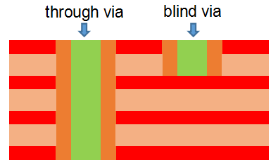
1. Thermal Vias,They can be mechanically drilled blind or through vias.
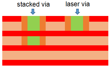
2. Laser, stacked micro-Vias, become more common, especially with low i/o pitch components.
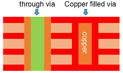
3. Coppr filled via
4. The better heat dissipation is the use of a local Cu-Coin. This can be a Bonded Cu-Coin, Press-Fit Cu-Coin or Embedded Cu-Coin.
Weller’s of copper coin embedded PCB capability
| Copper coin’s thickness | Unit (mm) |
| Coin material | Red copper |
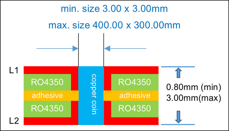
| Min. | 0.80 |
| Max. | 3.00 |
Remark: The adhesive in above stack up can be thermally conductive but not electrically.
| Copper coin’s szie | Unit (mm) |
| Min. | 3.00 x 3.00 |
| Max. | 400.00 x 300.00 (anyway, less than exact PCB size) |
Remark: The adhesive in above stack up can be thermally conductive but not electrically.
| Copper coin’s clearance | Unit (mm) |
| Min. | 1.00 |
| Max. | 1.00 |
Three key points of copper coin embedded in Rogers laminate material
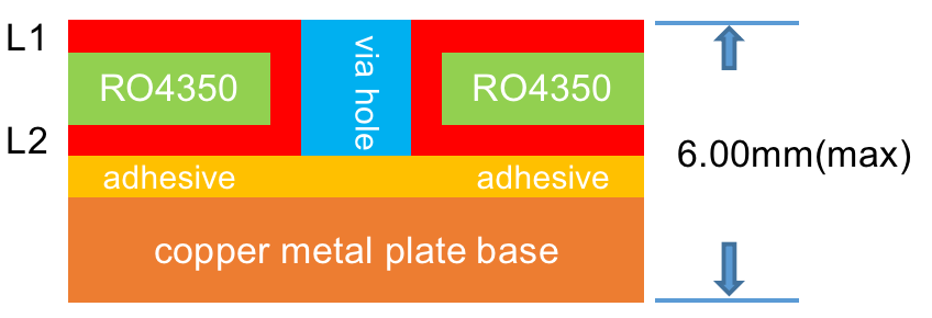
| 779Key point 1. Need 2 pcs core at least, for the purpse of adhesive sticking to copper coin.(refer below picture). we must need 2 cores, the reason is that: we use 2 cores to fill glue which can stick the embedded copper coin togetherly; or else the copper coin can not be stickedwith each other without any glue. |
| Key point 2. Total thickness of 2 pcs of core: 0.8mm (min) |
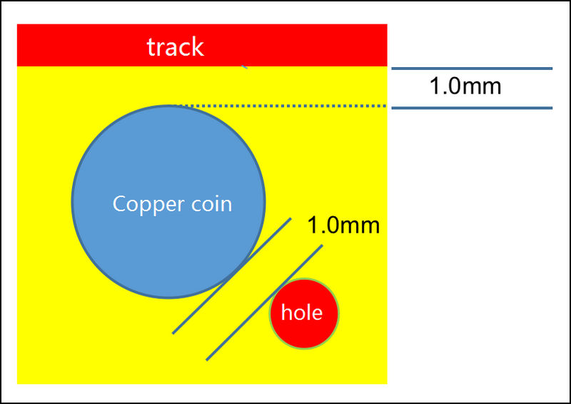
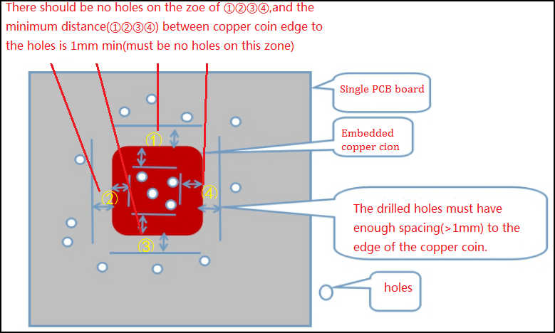
| Key point 3. The spacing between drilled holes to the edge of the copper coin must be no less than 1.0mm |
Stack up proposal for Hybrid PCB with rogers+copper plate base.
Copper metal plate base is a good option to transit the heat of Rogers PCBa.But the final PCB thickness is 6.0mm (max). The thickness more than 6.0mm will take challenge to laiminate press process.
Remark: The adhesive in above stack up can be thermally conductive but not electrically.
