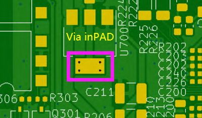
Via in Pad PCB Design
Via in pad is the design practice of placing a via in the copper landing pad of a component. Compared to standard PCB via routing, via in pad allows a design to use smaller component pitch sizes and further reduce the PCBs overall size. With component manufactures pushing smaller parts every year and the demand … Continued